ML9041A データシートの表示(PDF) - Oki Electric Industry
部品番号
コンポーネント説明
メーカー
ML9041A Datasheet PDF : 64 Pages
| |||
OKI Semiconductor
PEDL9041A-02
ML9041A-xxA/xxB
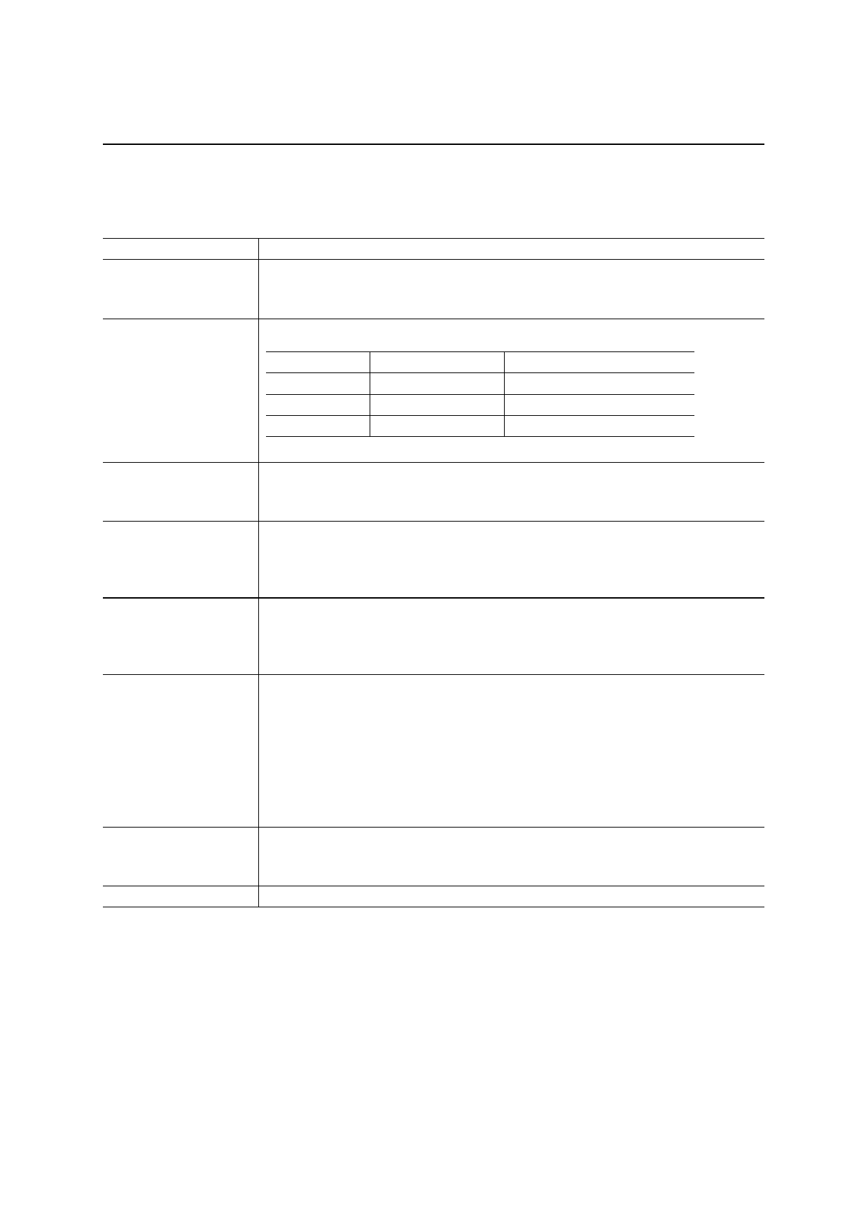
PIN DESCRIPTIONS
Symbol
R/W
RS0, RS1
E
DB0 to DB3
DB4 to DB7
OSC1
OSC2
OSCR
COM1 to COM17
SEG1 to SEG100
Description
The input pin with a pull-up resistor to select Read (“H”) or Write (“L”) in the Parallel I/F
Mode.
This pin should be open in the Serial l/F Mode.
The input pins with a pull-up resistor to select a register in the Parallel l/F Mode.
RS1
RS0
Name of register
H
H
Data register
H
L
Instruction register
L
L
Expansion Instruction register
This pin should be open in the Serial I/F Mode.
The input pin for data input/output between the CPU and the ML9041A and for
activating instructions in the Parallel l/F Mode.
This pin should be open in the Serial l/F Mode.
The input/output pins to transfer data of lower-order 4 bits between the CPU and the
ML9041A in the Parallel l/F Mode. The pins are not used for the 4-bit interface and
serial interface.
Each pin is equipped with a pull-up resistor, so this pin should be open when not used.
The input/output pins to transfer data of upper 4 bits between the CPU and the
ML9041A in the Parallel l/F Mode. The pins are not used for the serial interface.
Each pin is equipped with a pull-up resistor, so this pin should be open in the Serial I/F
Mode when not used.
The clock oscillation pins required for LCD drive signals and the operation of the
ML9041A by instructions sent from the CPU.
To input external clock, the OSC1 pin should be used. The OSCR and the OSC2 pins
should be open.
To start oscillation with an external resistor, the resistor should be connected between
the OSC1 and OSC2 pins. The OSCR pin should be open.
To start oscillation with an internal resistor, the OSC2 and OSCR pins should be
short-circuited outside the ML9041A. The OSC1 pin should be open.
The LCD common signal output pins.
For 1/9 duty, non-selectable voltage waveforms are output via COM10 to COM17. For
1/12 duty, non-selectable voltage waveforms are output via COM13 to COM17.
The LCD segment signal output pins.
4/64
Share Link: 