ML9041A データシートの表示(PDF) - Oki Electric Industry
部品番号
コンポーネント説明
メーカー
ML9041A Datasheet PDF : 64 Pages
| |||
OKI Semiconductor
PEDL9041A-02
ML9041A-xxA/xxB
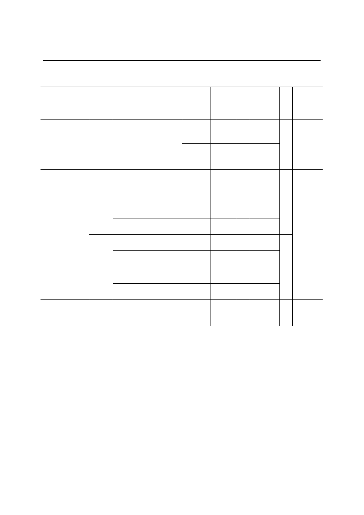
Parameter
Voltage Multiplier
Input Voltage
Voltage Multiplier
Output Voltage
Maximum and
minimum LCD
drive voltages
when internal
variable resistors
are used. Note 8
Symbol
VMUL
V5OUT
VLCD
MAX
VLCD
MIN
Condition
(GND = 0 V, VDD = 2.7 to 5.5 V, Ta = –40 to +85°C)
Min. Typ. Max. Unit Applicable
pins
Note 7
2.7
VDD = 2.7 V, VIN = 0 V
f = 125 kHz
1/5 bias 4.1
A capacitor for the voltage
multiplier = 1 to 4.7 µF
No load
1/4 bias 3.9
BE = “H”
VDD = 5 V, V5IN = –2 V, 1/5 bias,
6.6
Contrast data: 1F, No load
VDD = 5 V, V5IN = –2 V, 1/4 bias,
6.6
Contrast data: 1F, No load
VDD = 4.1 V, V5IN = 0 V, 1/5 bias,
3.8
Contrast data: 1F, No load
VDD = 3.9 V, V5IN = 0 V, 1/4 bias,
3.6
Contrast data: 1F, No load
VDD = 5 V, V5IN = –2 V, 1/5 bias,
4.0
Contrast data: 00, No load
VDD = 5 V, V5IN = –2 V, 1/4 bias,
3.6
Contrast data: 00, No load
VDD = 4.1 V, V5IN = 0 V, 1/5 bias, 2.2
Contrast data: 00, No load
VDD = 3.9 V, V5IN = 0 V, 1/4 bias, 1.9
Contrast data: 00, No load
—
3.5
V VDD–VIN
—
(VDD–VIN)
×2
V
—
(VDD–VIN)
×2
VDD–V5IN
—
—
—
—
—
—
—
—
—
4.6
—
4.2
—
2.8
—
2.5
V
VDD–V5
V
Bias Voltage for
Driving LCD
VLCD1
VLCD2
VDD–V5
1/5 bias 3.3 —
7.0
Note 9
V
V5
1/4 bias 3.3 —
7.0
Note 1:
Applied to the voltage drop occurring between any of the VDD, V1, V4 and V5 pins and any of the
common pins (COM1 to COM17) when the current of 4 µA flows in or flows out at one common
pin.
Also applied to the voltage drop occurring between any of the VDD, V2, V3A (V3B) and V5 pins and
any of the segment pins (SEG1 to SEG100) when the current of 4 µA flows in or flows out at one
common pin.
The current of 4 µA flows out when the output level is VDD or flows in when the output level is
V5.
Note 2: Applied to the current flowing into the VDD pin when the external clock (fOSC2 = fin = 270 kHz) is
fed to the internal Rf oscillation or OSC1 under the following conditions:
VDD = 5 V
GND = V5 = 0 V,
V1, V2, V3A (V3B) and V4: Open
E, SSR, CSR, and BE: “L” (fixed)
Other input pins: “L” or “H” (fixed)
Other output pins: No load
9/64
Share Link: 