ML9042 データシートの表示(PDF) - Oki Electric Industry
部品番号
コンポーネント説明
メーカー
ML9042 Datasheet PDF : 58 Pages
| |||
OKI Semiconductor
FEDL9042-01
ML9042-xx
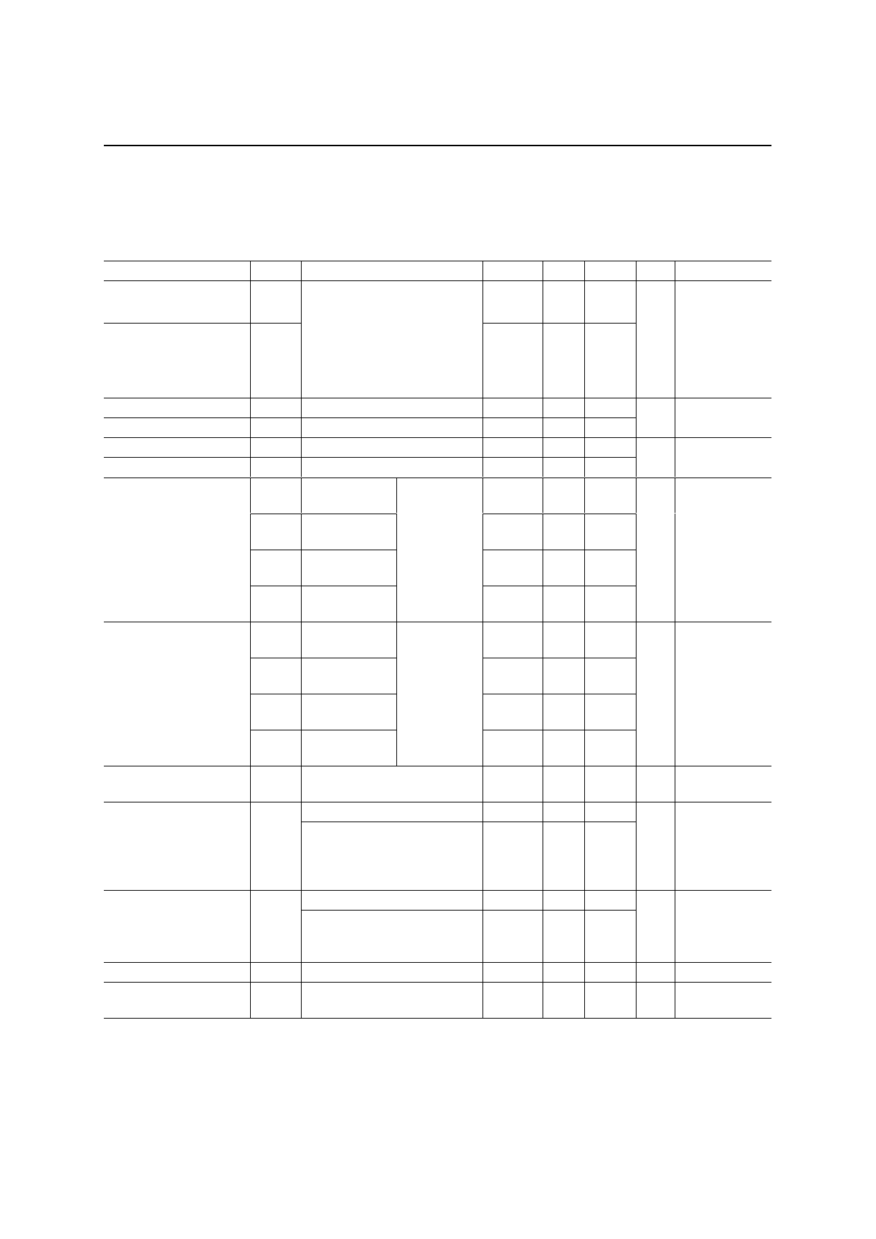
ELECTRICAL CHARACTERISTICS
DC Characteristics
Parameter
Symbol
Condition
(GND = 0 V, VDD = 2.7 to 5.5 V, Ta = –40 to +85°C)
Min. Typ. Max. Unit Applicable pin
“H” Input Voltage
VIH
“L” Input Voltage
VIL
0.8VDD —
VDD
RW/SI,
RS0/CSB, RS1,
E/SHTB,
—
V DB0(SO) to
0
— 0.2VDD
DB7, SP,
OSC1, BE,
ROM1S
“H” Output Voltage 1
“L” Output Voltage 1
“H” Output Voltage 2
“L” Output Voltage 2
VOH1
VOL1
VOH2
VOL2
IOH = –0.1 mA
IOL = +0.1 mA
IOH = –13 µA
IOL = +13 µA
0.9VDD
—
0.9VDD
—
—
—
—
0.1VDD
V
DB0(SO) to
DB7
——
— 0.1VDD V OSC2
VCH lOCH = –4 µA
V0–0.3
V0–
0.012
V0
COM Voltage Drop
VCMH
VCML
lOCMH = ±4 µA
lOCML = ±4 µA
V0 –GND = 5 V
Note 1
V1–0.3
V4–0.3
V1±
0.012
V4±
0.012
V1+0.3
V4+0.3
V
COM1 to
COM17
VCL lOCL = +4 µA
GND
GND+
GND+0.3
0.012
VSH lOSH = –4 µA
V0–0.3
V0–
0.012
V0
SEG Voltage Drop
VSMH
VSML
lOSMH = ±4 µA
lOSML = ±4 µA
V0 –GND = 5 V
Note 1
V2–0.3
V3–0.3
V2±
0.012
V3±
0.012
V2+0.3
V3+0.3
V
SEG1 to
SEG100
VSL lOSL = +4 µA
GND
GND+
GND+0.3
0.012
Input Leakage Current | IIL | VDD = 5 V, VI = 5 V or 0 V
—
—
1.0
µA
E/SHTB, BE,
SP, VIN
Input Current 1
VDD = 5 V, VI = GND
10
25 61
RW/SI,
| II1 |
VDD = 5 V, VI = VDD,
Excluding current flowing
through the pull-up resistor
and the output driving MOS
—
—
2.0
µA
RS0/CSB, RS1,
DB0(SO) to
DB7
Input Current 2
VDD = 5 V, VI = VDD
15
| II2 | VDD = 5 V, VI = GND
Excluding current flowing
—
through the pull-down resistor
45 105
—
2.0
µA T1, T2, T3
Supply Current
Oscillation Frequency
of External Resistor Rf
lDD VDD = 5 V
fosc1 Rf = 85 kΩ±2%
Note 2 —
Note 3 175
— 1.2 mA VDD–GND
270 400 kHz OSC1, OSC2
7/58
Share Link: 