ML9042 データシートの表示(PDF) - Oki Electric Industry
部品番号
コンポーネント説明
メーカー
ML9042 Datasheet PDF : 58 Pages
| |||
OKI Semiconductor
FEDL9042-01
ML9042-xx
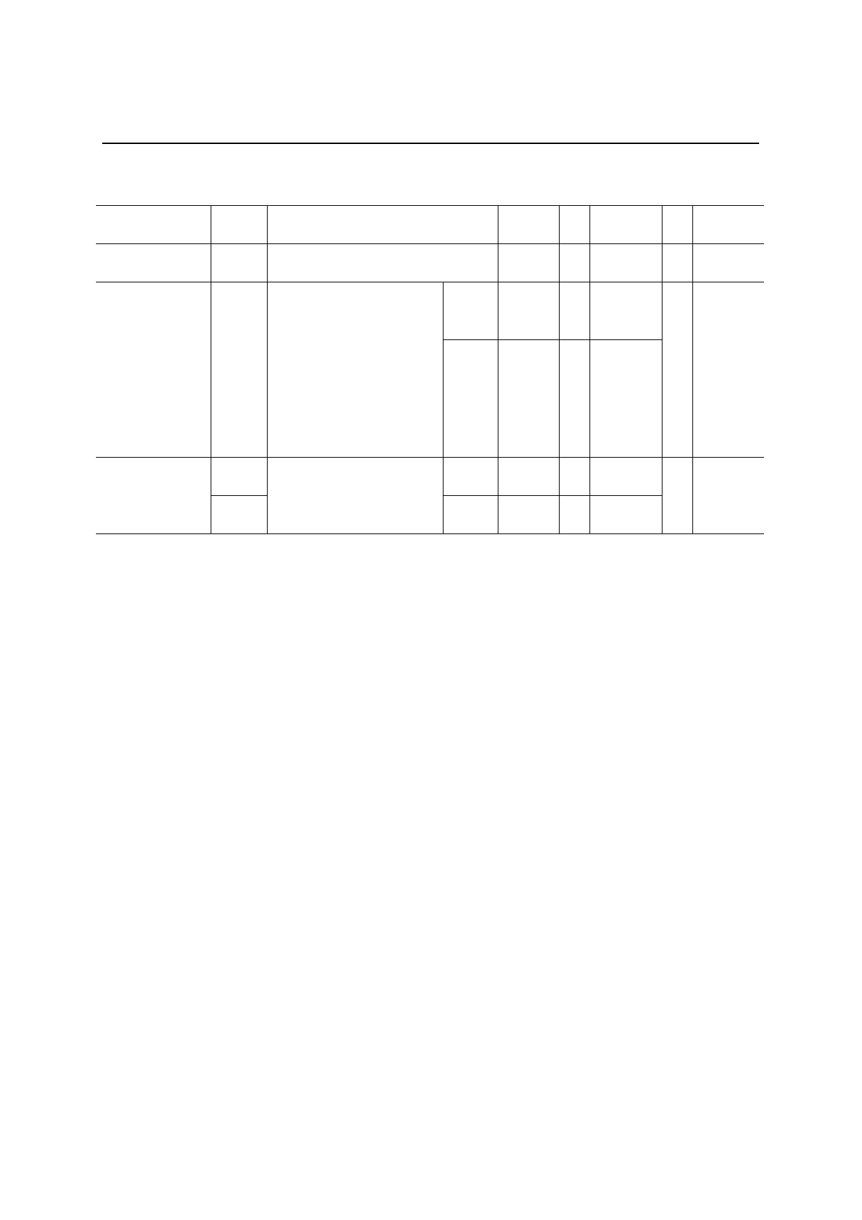
Parameter Symbol
Condition
Voltage Multiplier
Input Voltage
Voltage Multiplier
Output Voltage
VMUL
VOUT
Note 7
VDD = 2.7 V, VIN = 2.25 V
f = 175 kHz
A capacitor for the voltage
multiplier = 1 to 4.7 µF
VOUT load current = 54 µA
BE = “H”
Applied to LCD bias
resistance of 10 kΩ (TYP)
only
Bias Voltage for
Driving LCD
VLCD1
VLCD2
V0–GND
Note 8
(GND = 0 V, VDD = 2.7 to 5.5 V, Ta = –40 to +85°C)
Applicable
Min. Typ. Max. Unit
pins
1.8 — 2.75
V
VIN
1/5
bias
4.3
—
(VDD–VIN)
×2
1/4
bias
V
4.3
—
(VDD–VIN)
×2
VOUT
1/5
2.7 —
5.5
bias
V
V0
1/4
2.7 —
5.5
bias
Note 1:
Applied to the voltage drop occurring between any of the V0, V1, V4 and GND pins and any of
the common pins (COM1 to COM17) when the current of 4 µA flows in or flows out at one
common pin.
Also applied to the voltage drop occurring between any of the V0, V2, V3A (V3B) and GND pins
and any of the segment pins (SEG1 to SEG100) when the current of 4 µA flows in or flows out at
one segment pin.
The current of 4 µA flows out when the output level is VDD or flows in when the output level is
V5.
Note 2: Applied to the current flowing into the VDD pin when the external clock (fOSC2 = fin = 270 kHz) is
fed to the internal Rf oscillation or OSC1 under the following conditions:
VDD = V0 = 5 V
GND = 0 V,
V1, V2, V3A (V3B) and V4: Open
E/SHTB and BE: “L” (fixed)
Other input pins: “L” or “H” (fixed)
Other output pins: No load
9/58
Share Link: 