AD9060 データシートの表示(PDF) - Analog Devices
部品番号
コンポーネント説明
メーカー
AD9060 Datasheet PDF : 12 Pages
| |||
AD9060
MIL-STD-883 Compliance Information
The AD9060 devices are classified within Microcircuits Group
57, Technology Group D (bipolar A/D converters) and are con-
structed in accordance with MIL-STD-883. The AD9060 is
electrostatic sensitive and falls within electrostatic sensitivity
classification Class 1. Percent Defective Allowance (PDA) is
computed based on Subgroup 1 of the specified Group A test
list. Quality Assurance (QA) screening is in accordance with Al-
ternate Method A of Method 5005.
The following apply: Burn-In per 1015; Life Test per 1005;
Electrical Testing per 5004. (Note: Group A electrical testing
assumes TA = TC = TJ.) MIL-STD-883-compliant devices are
marked with “C” to indicate compliance.
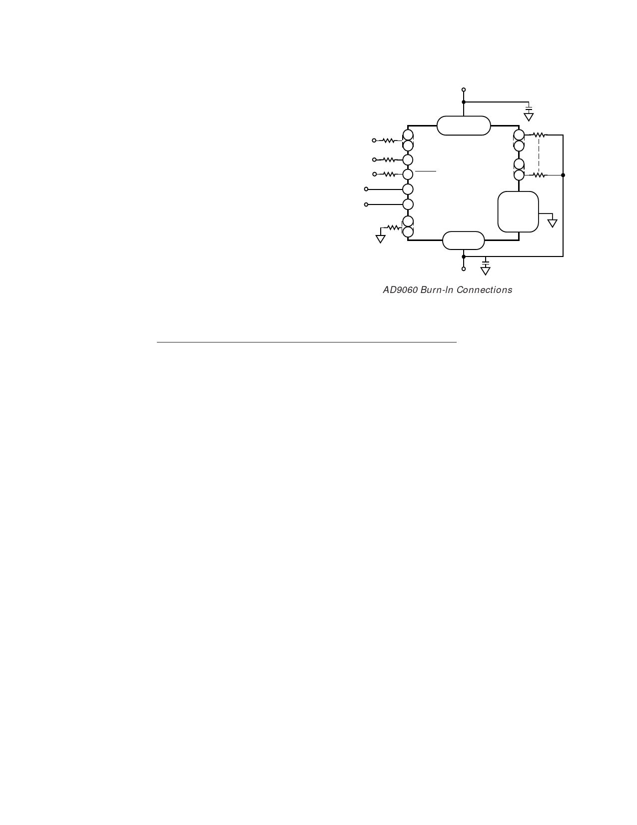
+ 5.0V
0.1 µF
AD1
AD2
AD3
+2V
–2V
100 Ω
3,6,15,30,33,34,
37,40,55,65,68
8
ANALOG IN
9
+V S
19
D0 – D4
23
510 Ω
510 Ω
510 Ω
14 ENCODE
13 ENCODE
12 +V REF
AD9060
D5 – D 9 46
51
510 Ω
4,5,17,
56 –VREF
GROUND
18,25,27,
31,32,36,
510 Ω
59 LSB INVERT
MSB
–VS
61 INVERT
2,16,28,29,35,
38,39,43,
45,52,53,66,67
41,42,54,64
STATIC: AD1 = –2V; AD 2 = ECL HIGH
AD3 = ECL LOW
DYNAMIC: AD1 = ±2V TRIANGLE WAVE
AD2,AD3 = ECL PULSE TRAIN
–5.2V
0.1µF
AD9060 Burn-ln Connections
THEORY OF OPERATION
Refer to the AD9060 block diagram. As shown, the AD9060
uses a modified “flash,” or parallel, A/D architecture. The ana-
log input range is determined by an external voltage reference
(+VREF and –VREF), nominally ± 1.75 V. An internal resistor
ladder divides this reference into 512 steps, each representing
two quantization levels. Taps along the resistor ladder (1/4REF,
1/2REF and 3/4REF) are provided to optimize linearity. Rated
performance is achieved by driving these points at 1/4, 1/2 and
3/4, respectively, of the voltage reference range.
The A/D conversion for the nine most significant bits (MSBs) is
performed by 512 comparators. The value of the least signifi-
cant bit (LSB) is determined by a unique interpolation scheme
between adjacent comparators. The decoding logic processes
the comparator outputs and provides a 10-bit code to the out-
put stage of the converter.
Flash architecture has an advantage over other A/D architec-
tures because conversion occurs in one step. This means the
performance of the converter is limited primarily by the speed
and matching of the individual comparators. In the AD9060, an
innovative interpolation scheme takes advantage of flash archi-
tecture but minimizes the input capacitance, power and device
count usually associated with that method of conversion.
These advantages occur because of using only half the normal
number of input comparator cells to accomplish the conversion.
In addition, a proprietary decoding scheme minimizes error
codes. Input control pins allow the user to select from among
Binary, Inverted Binary, Twos Complement and Inverted Twos
Complement coding (see AD9060 Truth Table).
APPLICATIONS
Many of the specifications used to describe analog/digital con-
verters have evolved from system performance requirements in
these applications. Different systems emphasize particular speci-
fications, depending on how the part is used. The following ap-
plications highlight some of the specifications and features that
make the AD9060 attractive in these systems.
Wideband Receivers
Radar and communication receivers (baseband and direct IF
digitization), ultrasound medical imaging, signal intelligence and
spectral analysis all place stringent ac performance requirements
on analog-to-digital converters (ADCs). Frequency domain
characterization of the AD9060 provides signal-to-noise ratio
(SNR) and harmonic distortion data to simplify selection of the
ADC.
Receiver sensitivity is limited by the Signal-to-Noise Ratio (SNR)
of the system. The SNR for an ADC is measured in the fre-
quency domain and calculated with a Fast Fourier Transform
(FFT). The SNR equals the ratio of the fundamental compo-
nent of the signal (rms amplitude) to the rms value of the
“noise.” The noise is the sum of all other spectral components,
including harmonic distortion but excluding dc.
Good receiver design minimizes the level of spurious signals in
the system. Spurious signals developed in the ADC are the result
of imperfections in the device transfer function (nonlinearities,
delay mismatch, varying input impedance, etc.). In the ADC,
these spurious signals appear as Harmonic Distortion. Harmonic
Distortion is also measured with an FFT and is specified as the
ratio of the fundamental component of the signal (rms ampli-
tude) to the rms value of the worst case harmonic (usually the
2nd or 3rd).
–6–
REV. A
Share Link: 