MP1541 データシートの表示(PDF) - Monolithic Power Systems
部品番号
コンポーネント説明
メーカー
MP1541 Datasheet PDF : 8 Pages
| |||
MP1541 – 1.3MHZ BOOST CONVERTER
PIN FUNCTIONS
Pin # Name Function
1
SW
Power Switch Output. SW is the drain of the internal MOSFET switch. Connect the power
inductor and output rectifier to SW. SW can swing between GND and 22V.
2 GND Ground.
3
FB Feedback Input. FB voltage is 1.25V. Connect a resistor divider to FB.
Regulator On/Off Control Input. A high input at EN turns on the converter, and a low input turns
4
EN it off. When not used, connect EN to the input source for automatic startup. The EN pin cannot
be left floating.
5
IN Input Supply Pin. Must be locally bypassed.
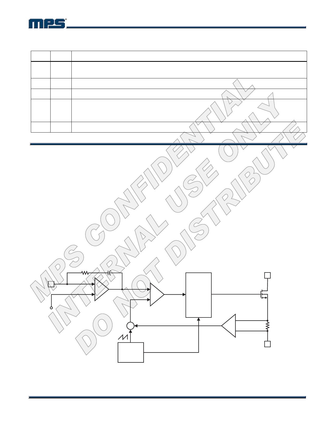
OPERATION
The MP1541 uses a fixed frequency, peak current
mode boost regulator architecture to regulate
voltage at the feedback pin. The operation of the
MP1541 can be understood by referring to the
block diagram of Figure 1. At the start of each
oscillator cycle the MOSFET is turned on through
the control circuitry. To prevent sub-harmonic
oscillations at duty cycles greater than 50 percent,
a stabilizing ramp is added to the output of the
current sense amplifier and the result is fed into
the negative input of the PWM comparator. When
this voltage equals the output voltage of the error
amplifier the power MOSFET is turned off. The
voltage at the output of the error amplifier is an
amplified version of the difference between the
1.25V bandgap reference voltage and the
feedback voltage. In this way the peak current
level keeps the output in regulation. If the
feedback voltage starts to drop, the output of the
error amplifier increases. This results in more
current to flow through the power MOSFET, thus
increasing the power delivered to the output.
The MP1541 has internal soft start to limit the
amount of input current at startup and to also
limit the amount of overshoot on the output. The
current limit is increased by a fourth every 40µs
giving a total soft start time of 120µs.
FB 3
1.25V
RC
CC
-
+
ERROR
AMPLIFIER
+
-
PWM
COMPARATOR
+
1.3MHz
OSC
CONTROL
LOGIC
+
-
CURRENT
SENSE
AMPLIFIER
SW
1
M1
2
GND
Figure 1—Functional Block Diagram
MP1541-F01-BD01
MP1541Rev.1.2
www.MonolithicPower.com
4
3/20/2006
MPS Proprietary Information. Unauthorized Photocopy and Duplication Prohibited.
© 2006 MPS. All Rights Reserved.
Share Link: 