MPC9774 データシートの表示(PDF) - Motorola => Freescale
部品番号
コンポーネント説明
メーカー
MPC9774 Datasheet PDF : 16 Pages
| |||
MPC9774
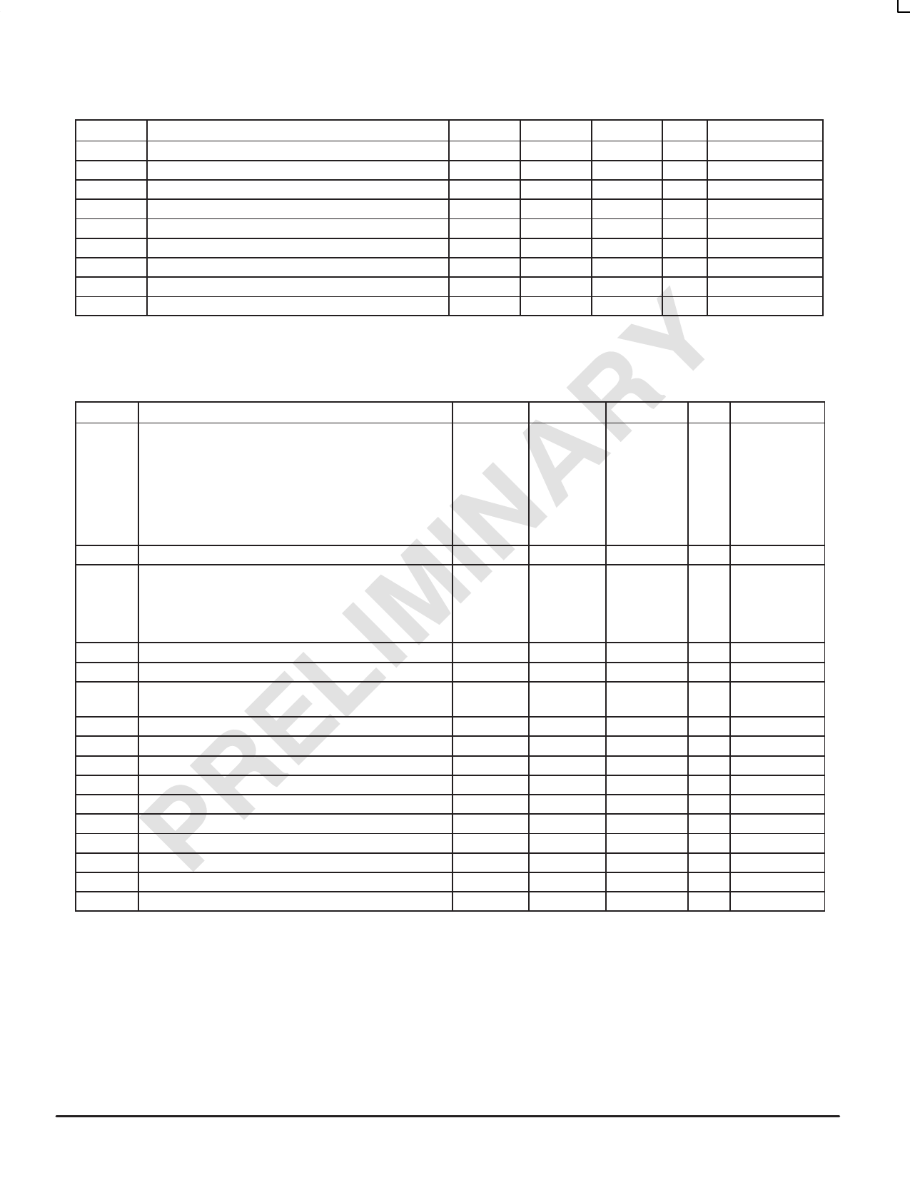
Table 9. DC Characteristics (VCC = 2.5V ± 5%, TA = 0°C to + 85°C)
Symbol
Characteristics
Min
Typ
Max
Unit
Condition
VCC_PLL PLL supply voltage
2.325
VCC
V LVCMOS
VIH
Input high voltage
1.7
VCC + 0.3 V
LVCMOS
VIL
VOH
Input low voltage
Output High Voltage
-0.3
0.7
V LVCMOS
1.8
V
IOH =-15 mAa
VOL
ZOUT
IIN
Output Low Voltage
Output impedance
Input Currentb
17 - 20
0.6
±200
V
IOL = 15 mA
W
µA VIN = VCC or GND
ICC_PLL Maximum PLL Supply Current
2.0
5.0
mA VCCA Pin
ICC
Maximum Quiescent Supply Current
1.0
mA All VCC Pins
a. The MPC9774 is capable of driving 50Ω transmission lines on the incident edge. Each output drives one 50Ω parallel terminated
transmission line to a termination voltage of VTT. Alternatively, the device drives up to two 50Ω series terminated transmission lines per
output.
b. Inputs have pull-down or pull-up resistors affecting the input current.
Table 10. AC Characteristics (VCC = 2.5V ± 5%, TA = 0°C to + 85°C)a b
Symbol
Characteristics
Min
Typ
Max
Unit Condition
fref
Input reference frequency
÷8 feedback
25.0
÷12 feedback
16.6
÷16 feedback
12.5
÷24 feedback
8.33
÷32 feedback
6.25
÷48 feedback
4.16
50.0
MHz PLL locked
33.3
MHz
25.0
MHz
16.6
MHz
12.5
MHz
8.3
MHz
Input reference frequency in PLL bypass modec
fVCO
VCO frequency ranged
200
fMAX Output Frequency
÷4 output
50.0
÷8 output
25.0
÷12 output
16.6
÷16 output
12.5
÷24 output
8.33
TBD
400
100.0
50.0
33.3
25.0
16.6
MHz
MHz
MHz
MHz
MHz
MHz
MHz
PLL bypass
PLL locked
frefDC
tr, tf
Reference Input Duty Cycle
CCLKx Input Rise/Fall Time
40
60
%
1
ns 0.7 to 1.7V
t(∅)
Propagation Delay (static phase offset)
CCLKx or PCLK to FB_IN
±150
ps PLL locked
tsk(O)
DC
Output-to-output Skewe
Output duty cycle
300
ps
45
50
55
%
tr, tf
tPLZ, HZ
tPZL, LZ
tJIT(CC)
tJIT(PER)
tJIT(∅)
BW
Output Rise/Fall Time
Output Disable Time
Output Enable Time
Cycle-to-cycle jitter
Period Jitter
I/O Phase Jitter
PLL closed loop bandwidthg
0.1
RMS (1 σ)f
RMS (1 σ)
RMS (1 σ)
TBD
TBD
TBD
1.0
10
10
TBD
ns 0.6 to 1.8V
ns
ns
ps
ps
ps
kHz
tLOCK Maximum PLL Lock Time
10
ms
a. All AC characteristics are design targets and subject to change upon device characterization.
b. AC characteristics apply for parallel output termination of 50Ω to VTT.
c. In bypass mode, the MPC9774 divides the input reference clock.
d. The input reference frequency must match the VCO lock range divided by the total feedback divider ratio: fref = fVCO ÷ (M ⋅ VCO_SEL).
e. See application section for part-to-part skew calculation.
f. See application section for a jitter calculation for other confidence factors than 1 σ.
g. -3 dB point of PLL transfer characteristics.
TIMING SOLUTIONS
7
MOTOROLA
Share Link: 