MPC9446ACR2 データシートの表示(PDF) - Integrated Device Technology
部品番号
コンポーネント説明
メーカー
MPC9446ACR2 Datasheet PDF : 12 Pages
| |||
MPC9446 Data Sheet
3.3V AND 2.5V LVCMOS CLOCK FANOUT BUFFER
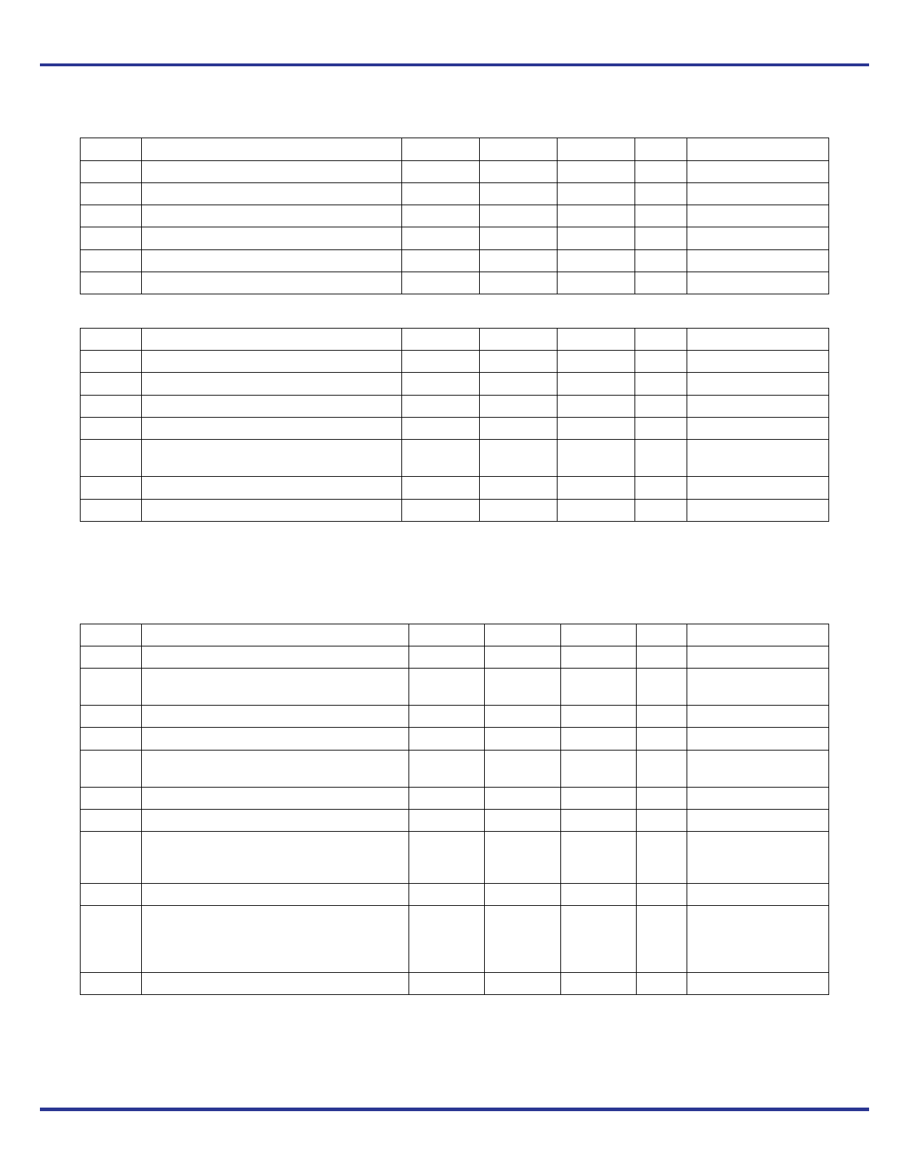
Table 5. General Specifications
Symbol
Characteristics
VTT Output Termination Voltage
MM ESD Protection (Machine Model)
HBM ESD Protection (Human Body Model)
LU Latch-Up Immunity
CPD Power Dissipation Capacitance
CIN Input Capacitance
Min
200
2000
200
Typ
VCC 2
10
4.0
Max
Unit
Condition
V
V
V
mA
pF Per output
pF
Table 6. DC Characteristics (VCC = VCCA = VCCB = VCCC = 3.3 V ± 5%, TA = –40°C to +85°C)
Symbol
Characteristics
Min
Typ
Max
Unit
Condition
VIH Input High Voltage
VIL Input Low Voltage
IIN
Input Current(1)
VOH Output High Voltage
VOL Output Low Voltage
ZOUT
ICCQ(3)
Output Impedance
Maximum Quiescent Supply Current
2.0
–0.3
2.4
14 – 17
VCC + 0.3
0.8
200
0.55
0.30
2.0
V LVCMOS
V LVCMOS
A VIN = GND or VIN = VCC
V
IOH = –24 mA(2)
V
IOL = 24 mA(2)
V IOL = 12 mA
mA All VCC Pins
1. Input pull-up / pull-down resistors influence input current.
2. The MPC9446 is capable of driving 50 transmission lines on the incident edge. Each output drives one 50 parallel terminated
transmission line to a termination voltage of VTT. Alternatively, the device drives up to two 50 series terminated transmission lines.
3. ICCQ is the DC current consumption of the device with all outputs open and the input in its default state or open.
Table 7. AC Characteristics (VCC = VCCA = VCCB = VCCC = 3.3 V ± 5%, TA = –40°C to +85°C)(1)
Symbol
Characteristics
Min
fref
fMAX
Input Frequency
Maximum Output Frequency
0
1 output
0
2 output
0
Typ
Max
Unit
Condition
250(2)
MHz
250(2)
125
MHz FSELx = 0
MHz FSELx = 1
tP, REF Reference Input Pulse Width
1.4
tr, tf CCLK Input Rise/Fall Time
tPLH Propagation Delay
tPHL
CCLK0,1 to any Q
2.2
CCLK0,1 to any Q
2.2
tPLZ, HZ Output Disable Time
tPZL, LZ Output Enable Time
tsk(O)
Output-to-Output Skew
Within one bank
Any output bank, same output divider
Any output, Any output divider
1.0(3)
ns
ns 0.8 to 2.0 V
2.8
4.45
ns
2.8
4.2
ns
10
ns
10
ns
150
ps
200
ps
350
ps
tsk(PP)
tSK(P)
Device-to-Device Skew
Output Pulse Skew(4)
2.25
ns
200
ps
DCQ Output Duty Cycle
tr, tf Output Rise/Fall Time
1 output
47
50
53
% DCREF = 50%
2 output
45
50
55
% DCREF = 25%–75%
0.1
1.0
ns 0.55 to 2.4 V
1. AC characteristics apply for parallel output termination of 50 to VTT.
2. The MPC9446 is functional up to an input and output clock frequency of 350 MHz and is characterized up to 250 MHz.
3. Violation of the 1.0 ns maximum input rise and fall time limit will affect the device propagation delay, device-to-device skew, reference input
pulse width, output duty cycle and maximum frequency specifications.
4. Output pulse skew tSK(P) is the absolute difference of the propagation delay times: | tPLH – tPHL |. Output duty cycle is frequency
dependent: DCQ = (0.5 ± tSK(P) • fOUT). For example at fOUT = 125 MHz the output duty cycle limit is 50% ± 2.5%.
MPC9446 REVISION 5 DECEMBER 21, 2012
4
©2012 Integrated Device Technology, Inc.
Share Link: 