TC1321VUATR データシートの表示(PDF) - Microchip Technology
部品番号
コンポーネント説明
メーカー
TC1321VUATR Datasheet PDF : 24 Pages
| |||
TC1321
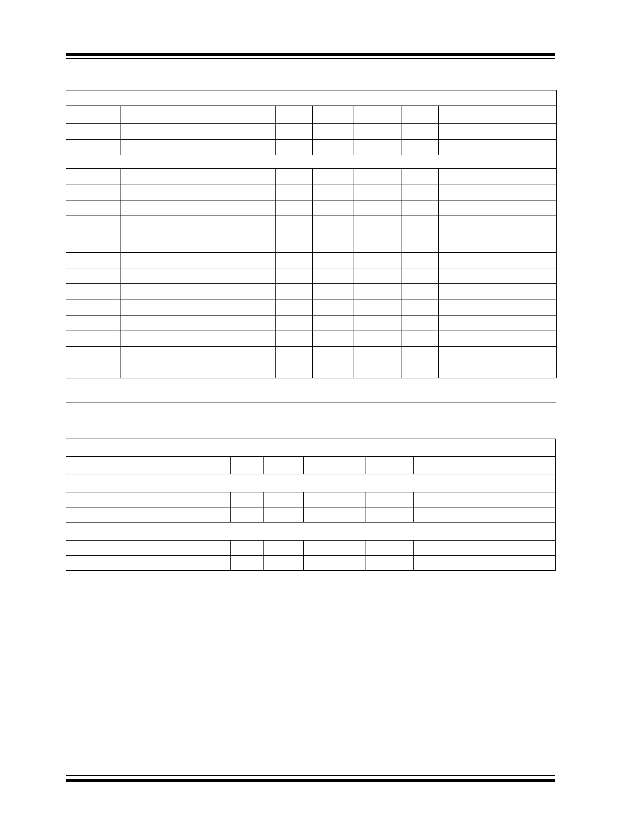
ELECTRICAL SPECIFICATIONS (CONTINUED)
Electrical Characteristics: VDD = 2.7V to 5.5V, -40°C TA +85°C, VREF = 1.2 V unless otherwise noted.
Symbol
Parameter
Min
Typ
Max
Unit
Test Conditions
CIN
Input Capacitance (SDA and SCL pins)
—
5
ILEAK
I/O Leakage
—
—
Serial Port AC Timing
fSMB
SMBus Clock Frequency
10
—
tIDLE
Bus Free Time Prior to New Transition
4.7
—
tH(START) START Condition Hold Time
4.0
—
tSU(START) START Condition Setup Time
4.7
—
0.4
pF
±1.0
µA
100
kHz
—
µs
—
µs
—
µs 90% SCL to 10% SDA
(for Repeated START
Condition)
tSU(STOP) STOP Condition Setup Time
4.0
—
—
tH-DATA
Data In Hold Time
100
—
—
tSU-DATA
Data In Setup Time
100
—
—
tLOW
Low Clock Period
4.7
—
—
tHIGH
High Clock Period
4
—
—
tF
SMBus Fall Time
—
—
300
tR
SMBus Rise Time
—
—
1000
tPOR
Power-on Reset Delay
—
500
—
Note 1: SDA and SCL must be connected to VDD or VSS.
2: Measured at VOUT 50 mV referred to VSS to avoid output buffer clipping.
µs
ns
ns
µs 10% to 10%
µs 90% to 90%
ns 90% to 10%
ns 10% to 90%
µs
VDD VPOR (Rising Edge)
TEMPERATURE CHARACTERISTICS
Electrical Specifications: VDD = 2.7V to 5.5V, -40°C TA +85°C, VREF = 1.2V unless otherwise noted.
Parameters
Symbol Min
Typ
Max
Units
Conditions
Temperature Ranges
Operating Temperature Range
TA
-40
—
+85
Storage Temperature Range
TA
-65
—
150
Thermal Package Resistances
Thermal Resistance, 8L SOIC
JA
—
149.5
—
Thermal Resistance, 8L MSOP
JA
—
211
—
°C
°C
°C/W
°C/W
DS21387C-page 4
2010 Microchip Technology Inc.
Share Link: 