MPX5100D データシートの表示(PDF) - Freescale Semiconductor
部品番号
コンポーネント説明
メーカー
MPX5100D
Freescale Semiconductor

MPX5100D Datasheet PDF : 16 Pages
| |||
PRESSURE (P1)/VACUUM (P2) SIDE IDENTIFICATION TABLE
Freescale designates the two sides of the pressure sensor
as the Pressure (P1) side and the Vacuum (P2) side. The
Pressure (P1) side is the side containing fluoro silicone gel
which protects the die from harsh media. The MPX pressure
sensor is designed to operate with positive differential
pressure applied, P1 > P2.
The Pressure (P1) side may be identified by using Table 3
below.
TABLE 3. PRESSURE (P1)/VACUUM (P2) SIDE IDENTIFICATION TABLE
Part Number
MPX5100A, MPX5100D
MPX5100DP
MPX5100AP, MPX5100GP
MPX5100GSX
MPXV5100GC6U
MPXV5100GC7U
MPXV5100DP
MPXV5100GP
Case Type
867
867C
867B
867F
482A
482C
1351
1369
Pressure (P1) Side Identifier
Stainless Steel Cap
Side with Part Marking
Side with Port Attached
Side with Port Attached
Side with Port Attached
Side with Port Attached
Side with Part Marking
Side with Port Attached
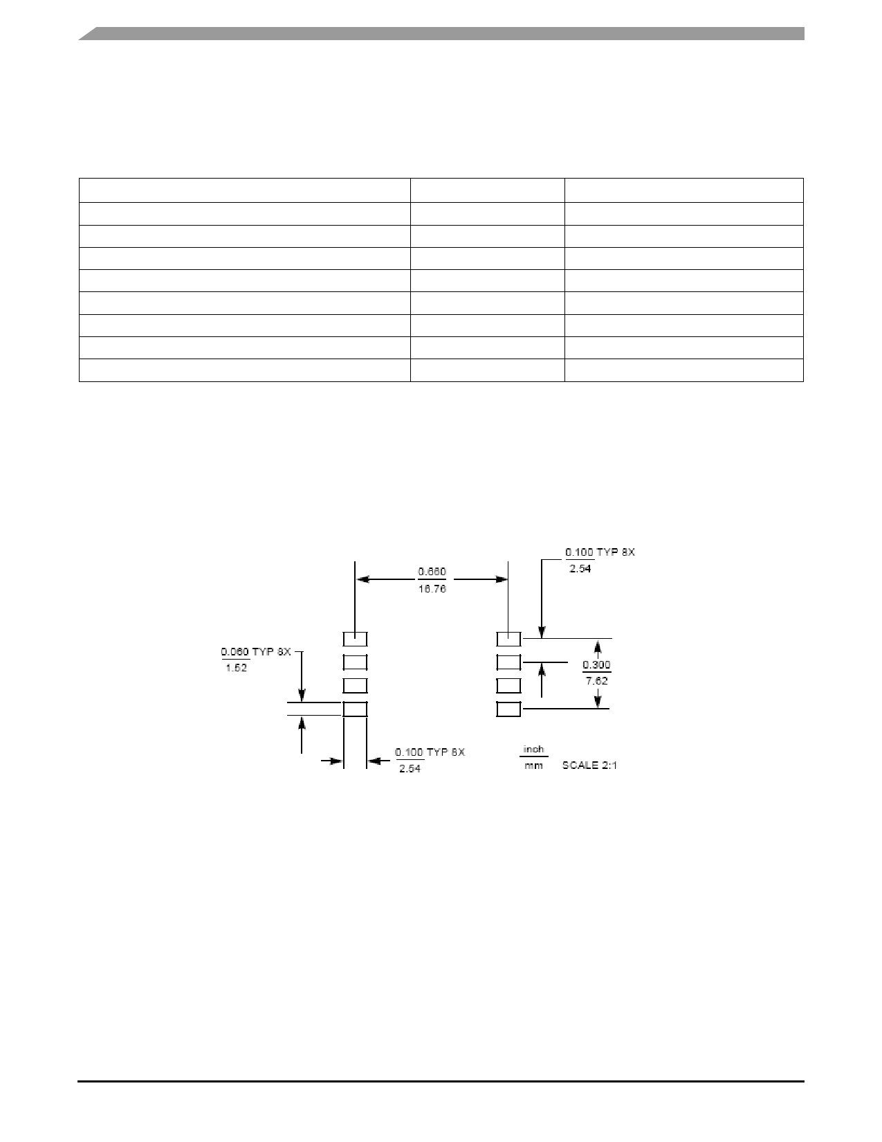
INFORMATION FOR USING THE SMALL OUTLINE PACKAGE
MINIMUM RECOMMENDED FOOTPRINT FOR SURFACE MOUNTED APPLICATIONS
Surface mount board layout is a critical portion of the total
design. The footprint for the surface mount packages must be
the correct size to ensure proper solder connection interface
between the board and the package. With the correct
footprint, the packages will self align when subjected to a
solder reflow process. It is always recommended to design
boards with a solder mask layer to avoid bridging and
shorting between solder
Figure 5. Small Outline Package Footprint
MPX5100
6
Sensors
Freescale Semiconductor
Share Link: