MR27V1652E データシートの表示(PDF) - Oki Electric Industry
部品番号
コンポーネント説明
メーカー
MR27V1652E
Oki Electric Industry

MR27V1652E Datasheet PDF : 15 Pages
| |||
OKI Semiconductor
FEDR27V1652E-01-02
MR27V1652E / OTP
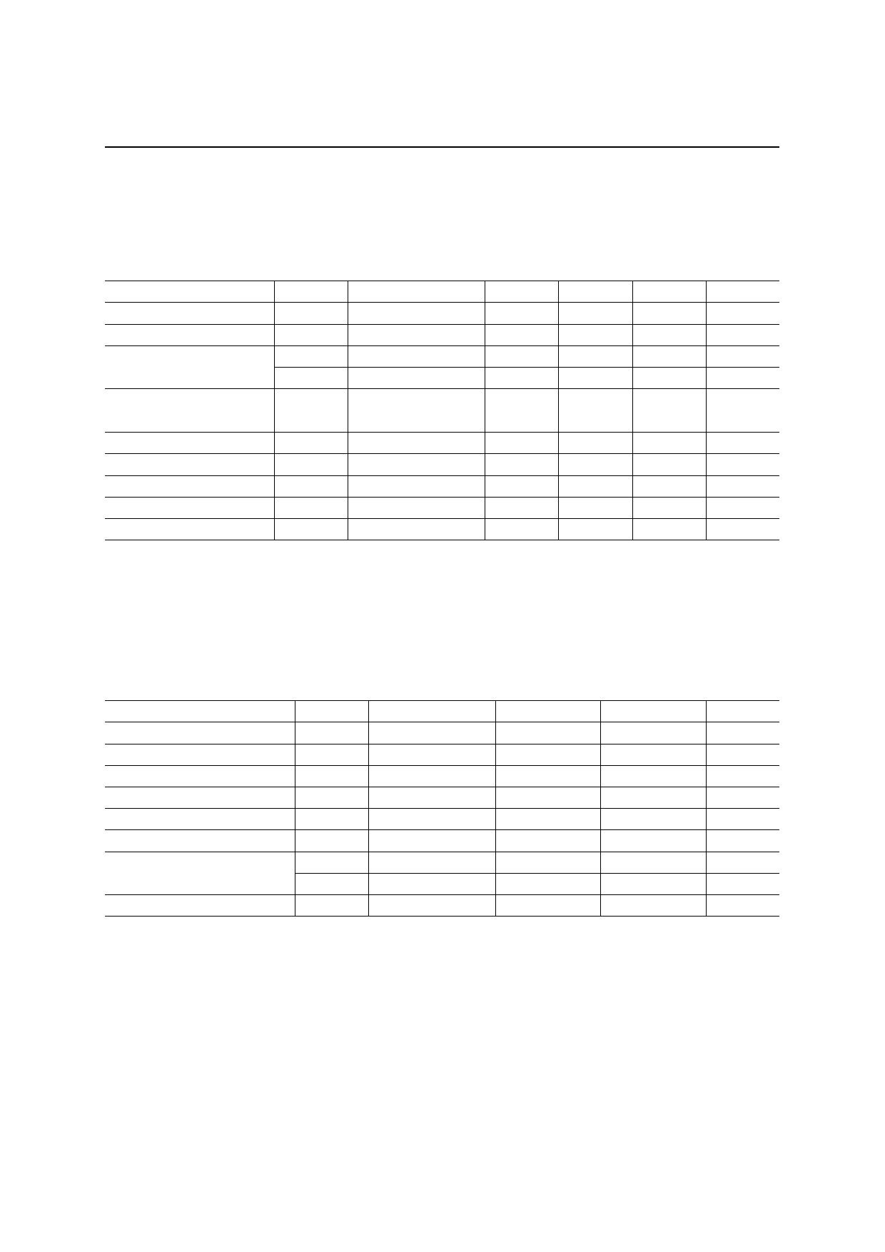
ELECTRICAL CHARACTERISTICS
DC Characteristics
parameter
Input leakage current
Output leakage current
VCC power supply current
(Standby)
VCC power supply current
(Read)
VPP power supply current
Input “H” level
Input “L” level
Output “H” level
Output “L” level
Symbol
ILI
ILO
ICCSC
ICCST
ICCA
IPP
VIH
VIL
VOH
VOL
Condition
VI = 0 to VCC
VO = 0 to VCC
CE = VCC
CE = VIH
CE = VIL, OE = VIH
tc = 100 ns
VPP = VCC
—
—
IOH = –400 µA
IOL = 2.1 mA
(VCC = 3.3 V ± 0.3 V, Ta = 0 to 70°C)
Min.
Typ.
Max.
Unit
—
—
10
µA
—
—
10
µA
—
—
50
µA
—
—
1
mΑ
—
—
100
mA
—
2.2
–0.5∗∗
2.4
—
—
10
µA
—
VCC+0.5∗
V
—
0.6
V
—
—
V
—
0.4
V
Voltage is relative to VSS.
∗ : Vcc+1.5V(Max.) when pulse width of overshoot is less than 10ns.
∗∗ : -1.5V(Min.) when pulse width of undershoot is less than 10ns.
AC Characteristics
Parameter
Address cycle time
Address access time
Page cycle time
Page access time
CE access time
OE access time
Output disable time
Output hold time
Symbol
tC
tACC
tPC
tPAC
tCE
tOE
tCHZ
tOHZ
tOH
Condition
—
CE = OE = VIL
—
—
OE = VIL
CE = VIL
OE = VIL
CE = VIL
CE = OE = VIL
(VCC = 3.3 V ± 0.3 V, Ta = 0 to 70°C)
Min.
Max.
Unit
100
—
ns
—
100
ns
30
—
ns
—
30
ns
—
100
ns
—
30
ns
0
30
ns
0
25
ns
0
—
ns
Measurement conditions
Input signal level-------------------------------- 0 V/3 V
Input timing reference level ------------------ 0.8 V/2.0 V
Output load -------------------------------------- 100 pF
Output timing reference level---------------- 0.8 V/2.0 V
5/15
Share Link: