MAX3676E データシートの表示(PDF) - Maxim Integrated
部品番号
コンポーネント説明
メーカー
MAX3676E Datasheet PDF : 16 Pages
| |||
622Mbps, 3.3V Clock-Recovery and
Data-Retiming IC with Limiting Amplifier
Note that the LOL monitor is only valid when a data
stream is present on the inputs to the MAX3676. As a
result, LOL does not detect a loss-of-power condition
resulting from a loss of the incoming signal. See the
Loss-of-Power Monitor section for this type of indicator.
Input and Output Terminations
The MAX3676 digital data and clock I/Os (DDI+, DDI-,
SDO+, SDO-, SCLK+, and SCLK-) are designed to
interface with PECL signal levels. It is important to bias
these ports appropriately. A circuit that provides a
Thevenin equivalent of 50Ω to VCC - 2V should be used
with fixed-impedance transmission lines for proper ter-
mination. Make sure that the differential outputs have
balanced loads.
The digital data input signals (DDI+ and DDI-) are dif-
ferential inputs to an emitter-coupled pair. As a result,
the MAX3676 can accept differential input signals as
low as 250mV. These inputs can also be driven single-
ended by externally biasing DDI- to the center of the
voltage swing.
The MAX3676’s performance can be greatly affected
by circuit board layout and design. Use good high-fre-
quency design techniques, including minimizing
ground inductance and using fixed-impedance trans-
mission lines on the data and clock signals. Power-sup-
ply decoupling should be placed as close to VCC as
possible. Take care to isolate the input from the output
signals to reduce feedthrough.
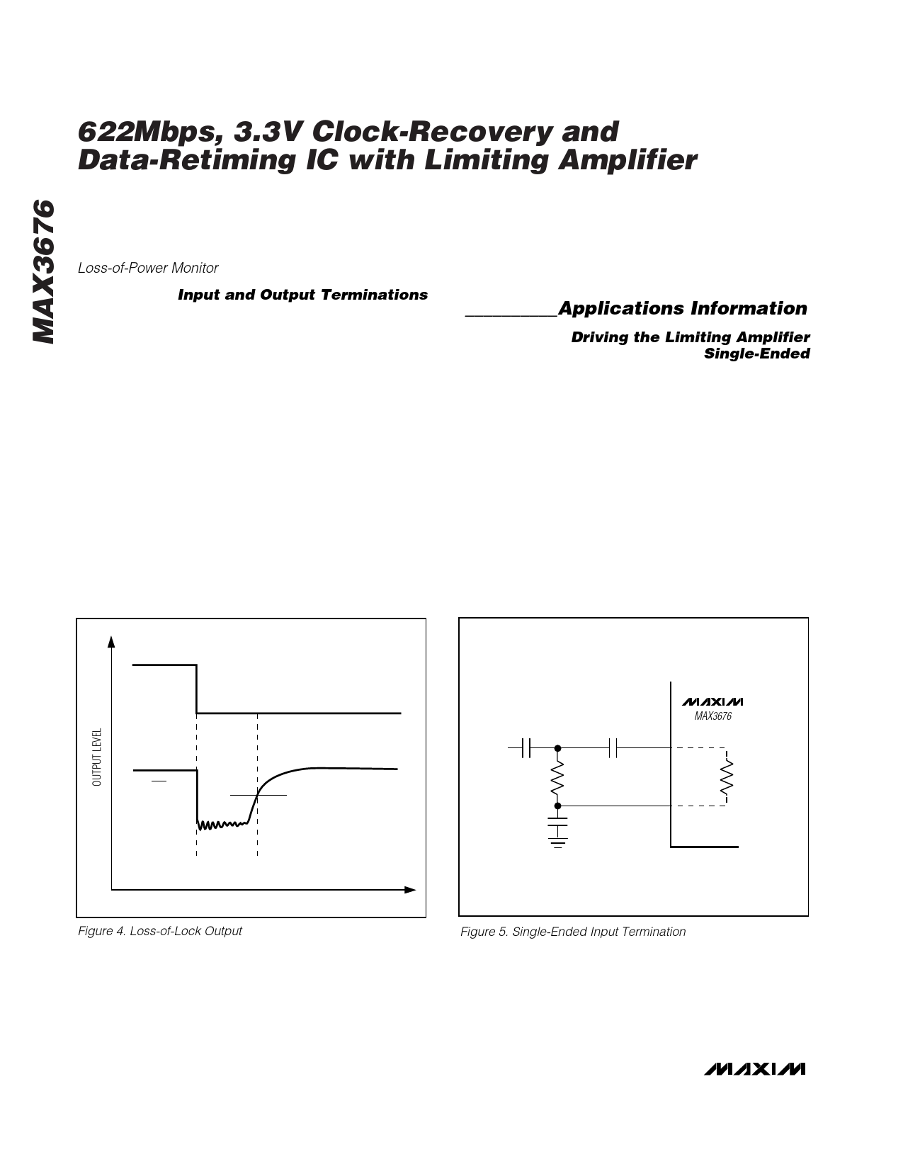
__________Applications Information
Driving the Limiting Amplifier
Single-Ended
There are three important requirements for driving the
limiting amplifier from a single-ended source (Figure 5):
1) There must be no DC-coupling to the ADI+ and ADI-
inputs. DC levels at these inputs disrupt the offset-
correction loop.
2) The terminating resistor RT (50Ω) must be referenced
to the ADI- input to minimize common-mode coupling
problems.
3) The low-frequency cutoff for the limiting amplifier
is determined by either CIN and the 2.5kΩ input
impedance or Cb/2 together with RT. With Cb = 0.22µF
and RT = 50Ω, the low-frequency cutoff is 29kHz.
LOP
LOL
NO DATA
ACQUIRE
LOCKED
TIME
Figure 4. Loss-of-Lock Output
Cb
0.22µF
CIN
5.6nF
ADI+
RT
50Ω
ADI-
Cb
0.22µF
MAX3676
2.5k
Figure 5. Single-Ended Input Termination
10 ______________________________________________________________________________________
Share Link: 