MSC1209 データシートの表示(PDF) - Oki Electric Industry
部品番号
コンポーネント説明
メーカー
MSC1209
Oki Electric Industry

MSC1209 Datasheet PDF : 16 Pages
| |||
¡ Semiconductor
MSC1209
FUNCTIONAL DESCRIPTION
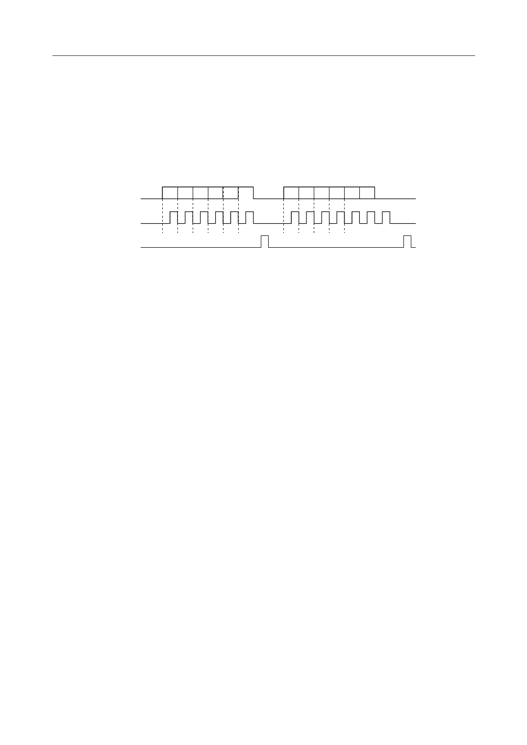
DATA Input
This device uses 10-bit dimming data (D1 to D10) and 84-bit segment data (S1 to S84). To transfer
these data, the mode bits (M0 and M1) must be sent after each of these data succeedingly. The
data transfer timing diagram is shown below.
DATA
CLOCK
LOAD
D1 D2 D10 M0 M1
S1 S2 S83 S84 M0 M1
Figure 1 Data Transfer Timing
M0 : Enable bit
M0 = "0": Indicates the data from the master IC.
M0 = "1": Indicates the data from the slave IC.
M1 : Mode specification bit
M1 = "1": Indicates that the data sent on ahead is dimming data.
M1 = "0": Indicates that the data sent on ahead is segment data.
D1 : LSB of dimming data
S1 : data for GRID1 of SEG1
S2 : data for GRID1 of SEG2
:
S42 : data for GRID1 of SEG42
S43 : data for GRID2 of SEG1
:
S84 : data for GRID2 of SEG42
Notes: 1. When the number of input data bits are larger, the data bits are pushed out in the
same order that they are input, and 86 bits of the data counted from the bit entered
last are used as valid data. (In the case of segment data)
2. When the number of input data bits are smaller, the data remaining in the shift
register before data transfer is shifted and used as valid data.
CLOCK Input
Data is shifted at the rising edge of the clock.
LOAD Input
The contents of the shift register are shifted in while the LOAD input is "H" level and latched at
"H" to "L" transition. This LOAD signal is regenerated in the VFD tube driver for the latch pulse
for dimming data and segment data. When 10-bit dimming data and 84-bit segment data have
been transferred, input the LOAD signal prior to the next clock.
9/15
Share Link: