4225 データシートの表示(PDF) - M.S. Kennedy Corporation
部品番号
コンポーネント説明
メーカー
4225 Datasheet PDF : 5 Pages
| |||
APPLICATION NOTES
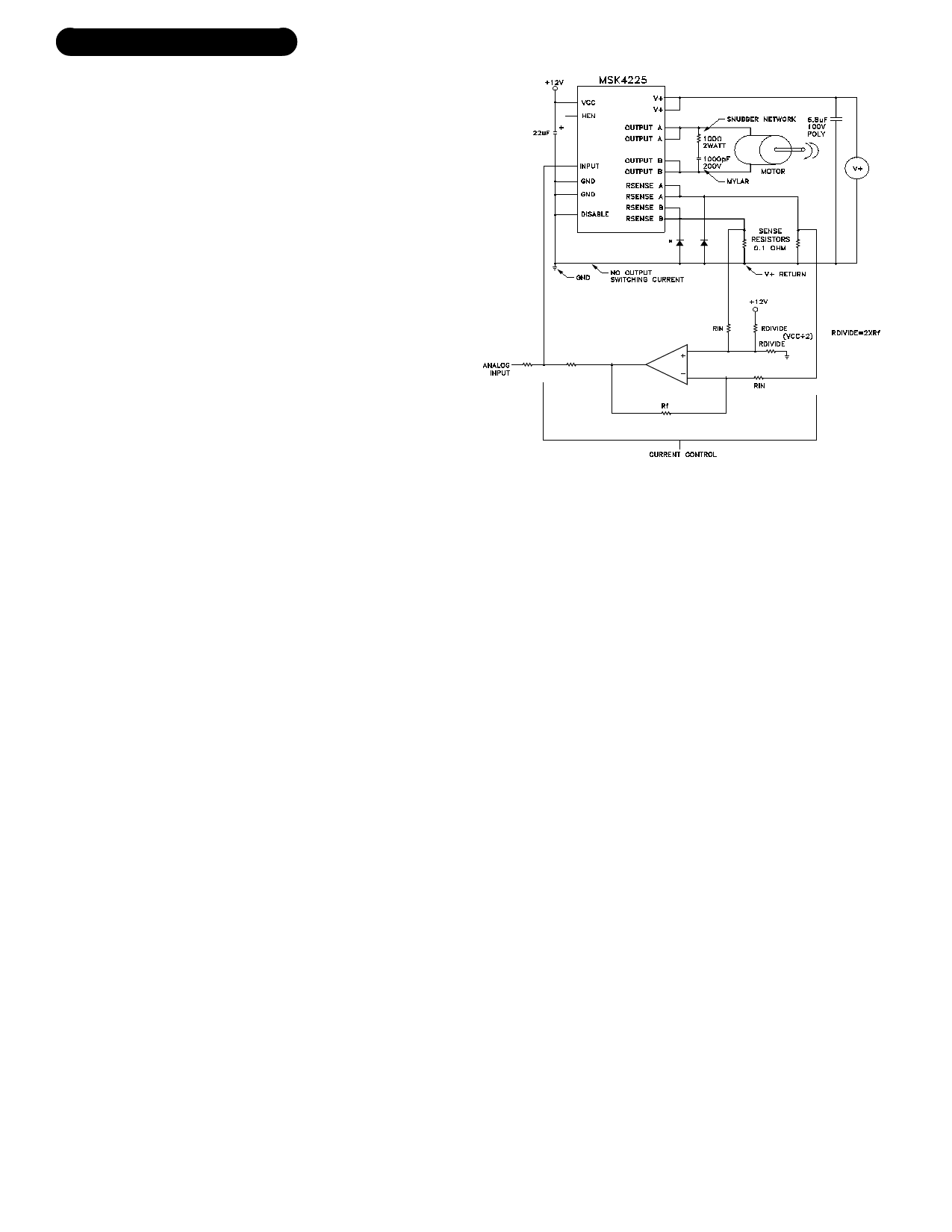
TYPICAL SYSTEM OPERATION
MSK 4225 PIN DESCRIPTIONS
VCC - Is the low voltage supply for powering internal logic
and drivers for the lowside and highside MOSFETS.
The supplies for the highside drivers are derived from this
voltage.
V+ - Is the higher voltage H-bridge supply. The MOSFETS
obtain the drive current from this supply pin. The voltage
on this pin is limited by the drive IC. The MOSFETS are
rated at 75 volts. Proper by-passing to GND with suffi-
cient capacitance to suppress any voltage transients, and
to ensure removing any drooping during switching, should
be done as close to the pins of the module as possible.
OUTPUT A - Is the output pin for one half of the bridge.
Decreasing the input voltage causes increasing duty cycles
at this output.
OUTPUT B - Is the output pin for the other half of the
bridge. Increasing the input voltage causes increasing
duty cycles at this output.
RSENSE A - Is the connection for the bottom of the A half
bridge. This can have a sense resistor connection to the
V+ return ground for current limit sensing, or can be con-
nected directly to ground. The maximum voltage on this
pin is ±2 volts with respect to GND.
RSENSE B - Is the connection for the bottom of the B half
bridge. This can have a sense resistor connection to the
V+ return ground for current limit sensing, or can be con-
nected directly to ground. The maximum voltage on this
pin is ±2 volts with respect to GND.
GND - Is the return connection for the input logic and Vcc.
INPUT - Is an analog input for controlling the PWM pulse
width of the bridge. A voltage lower than Vcc/2 will pro-
duce greater than 50% duty cycle pulses out of OUTPUT
A. A voltage higher than Vcc/2 will produce greater than
50% duty cycle pulses out of OUTPUT B.
DISABLE - Is the connection for disabling all 4 output
switches. DISABLE high overrides all other inputs. When
taken low, everything functions normally. An internal
pullup to Vcc will keep DISABLE high if left unconnected.
HEN - Is the connection for enabling the high side output
switches. When taken low, HEN overrides other inputs
and the high side switches remain off. When HEN is high
everything functions normally. An internal pullup to Vcc
will keep HEN high if left unconnected.
This is a diagram of a typical application of the MSK4225. The
design Vcc voltage is +12 volts and should have a good low ESR
bypass capacitor such as a tantalum electrolytic. The analog input
can be an analog speed control voltage from a potentiometer, other
analog circuitry or by microprocessor and a D/A converter. This
analog input gets pulled by the current control circuitry in the proper
direction to reduce the current flow in the bridge if it gets too high.
The gain of the current control amplifier will have to be set to
obtain the proper amount of current limiting required by the sys-
tem.
IN
Current sensing is done in this case by a 0.1 ohm sense resis-
tor to sense current from both legs of the bridge separately. It is
important to make the high current traces as big as possible to keep
inductance down. The storage capacitor connected to the V+ and
the module should be large enough to provide the high energy
pulse without the voltage sagging too far. A low ESR ceramic
capacitor or large polypropylene capacitor will be required. Mount
the capacitor as close to the module as possible. The connection
between GND and the V+ return should not be carrying any motor
current. The sense resistor signal is common mode filtered as nec-
essary to feed the limiting circuitry for the microprocessor. This
application will allow full four quadrant torque control for a closed
loop servo system.
A snubber network is usually required, due to the inductance in
the power loop. It is important to design the snubber network to
suppress any positive spikes above 70V and negative spikes be-
low -2V with respect to ground.
*There are certain inductive load situations that can possibly cause
a momentary shoot-through or cross-conduction condition in the
MSK4225. This shoot-through is approximately 100nSec long
and can be several amps, depending on the layout and impedence
of the bypassing circuit. Most bypassing and current sensing filter-
ing will usually eliminate the effects. However, in the case where it
is still present, or the sense resistor trace lengths are long, reverse-
biased ultra-fast recovery diodes or power schottky diodes from
RSENSE A and RSENSE B to power ground will minimize or elimi-
nate the situation.
3
Rev. B 11/04
Share Link: 