MSM6889RS データシートの表示(PDF) - Oki Electric Industry
部品番号
コンポーネント説明
メーカー
MSM6889RS Datasheet PDF : 21 Pages
| |||
¡ Semiconductor
MSM6889
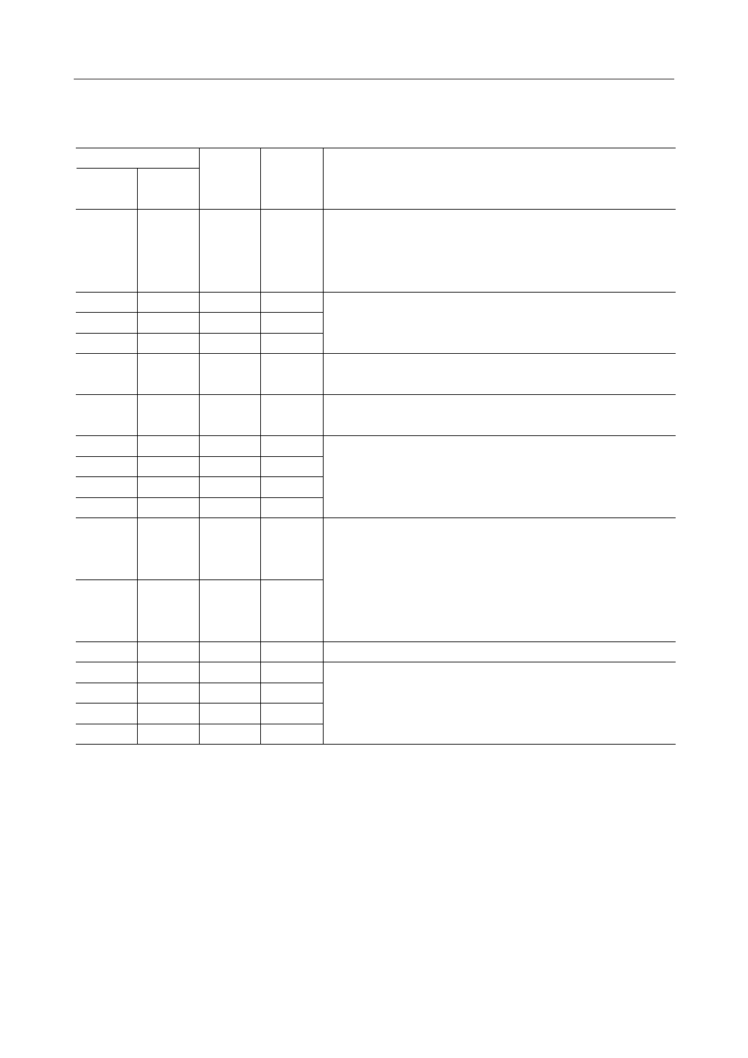
PIN DESCRIPTION
Pin Number
Name
I/O
RS
GS
Description
+5 V Power Supply (Analog Circuit).
When power is turned on or the power down mode is released, the
1
35
VA
—
device must be put into the PB tone transmit mode or PB tone
detect mode.
2
37
GAR
O Output, non-inverting input and inverting input pins of on-chip
3
39
AIN+
I
operational amplifier.
4
40
AIN–
I
No hybrid transformer is required by use of these pins. (See Fig. 2.)
Analog signal output.
5
41
AO
O
PB tone or modem transmit signal is output from this pin.
6
43
SG
O On-chip signal ground, having a potential of about +2.5 V.
7
44
GAT1
I
PB is the PB tone output and MOD is the modem signal output.
8
45
GAT2
O By connecting external resistors to GAT1 and GAT2 pins, signal level can
9
46
MOD
O be set at required values for the modem signal and
10
47
PB
O the PB tone that are output from AO, independently. (See Fig. 3.)
These pins are used to externally adjust the received carrier
11
50
VR1
O detect(CD) signal level.
The potential of VR1 to SG is about +1.1 V. The carrier
detect level can be set at the required value by a on-chip resistor
12
51
VR2
I
divider between VR1 and SG. The given potential to VR2 is set
about +0.88 V with high resistance inside the IC. (See Fig. 4.)
13
52
AG
— Analog Ground, 0 V.
14
53
PBG1
I*
Inputs used to specify PB tone to be sent.
15
54
PBG2
I*
PB1 to PB4 can be connected externally like 4-bit bus line. Data is
16
56
PBG3
I*
latched at the falling edge of TEN. (See Fig. 7 and Fig. 8.)
17
2
PBG4
I*
* Digital input pulled up by a high resistance inside the IC.
5/21
Share Link: 