MSM6889GS-K データシートの表示(PDF) - Oki Electric Industry
部品番号
コンポーネント説明
メーカー
MSM6889GS-K Datasheet PDF : 21 Pages
| |||
¡ Semiconductor
MSM6889
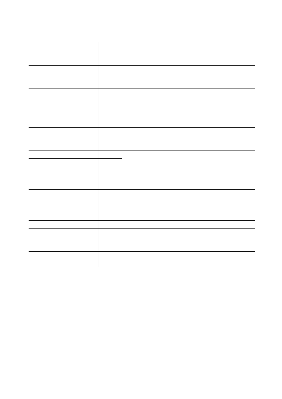
Pin Number
Name
I/O
RS
GS
Description
PB tone transmit enable.
18
3
TEN
I* PBG1 to PBG4 data are latched at the falling edge of TEN, and PB
tone is generated at digital "0" level. (See Fig. 7.)
Modem transmit serial data input.
19
4
TD
I* Data stream less than 300 bps should be input.
Digital "1" and "0" correspond to "Mark" and "Space" respectively.
20
6
RS
Request to send data input .
I*
While RS is at digital "0" level, modem transmit is enabled.
21
7
DG
— Digital Ground, 0 V.
Input used to select call progress tone (CPT) detect output
22
8
ICT1
I*
waveform. (See Fig. 9.)
23
9
ICT2
I* Used to check performance characteristics of the IC.
24
11
ICT3
I* Independent of operating mode. Leave these pins open.
25
12
MODE1
I*
Inputs used to specify operating mode.
26
13
MODE2
I*
(See Table 1.)
27
14
MODE3
I*
28
16
X1
3.579545 MHz crystal resonator should be connected to X1 and X2.
I
When applying external clock to the device, it should be connected
to X2 through the AC coupling capacitor of 100 pF and X1 has to be
29
17
X2
O
open.
30
19
CLK
O 3.579545 MHz clock output.
Modem receive serial data output.
31
20
RD
O Digital "1" and "0" correspond to "Mark" and "Space" respectively.
When CD (Carrier Detect) is off, RD is hold at "Mark" state.
32
22
CD
Carrier Detect output.
O
Digital "0" and "1" represent "Detect" and "No-detect" respectively.
* Digital input pulled up by a high resistance inside the IC.
6/21
Share Link: 