MSM6896 データシートの表示(PDF) - Oki Electric Industry
部品番号
コンポーネント説明
メーカー
MSM6896 Datasheet PDF : 43 Pages
| |||
¡ Semiconductor
MSM6895/6896
R1I, R2I, RPO
Receive preamplifier inputs and output.
R1I and R2I are for the inputs and RPO is for the output of the receive preamplifier. Normally,
R1I is connected via an AC-coupling capacitor to the CODEC analog output (CAO), and R2I is
used as the mixing signal input pin.
During initial setting, the RPO output is in non-signal state (VSG level), and speech signal,
RTONE1, RTONE2, FTONE, PB acknowledge tone, and side tone signal are output through
processor control. And if the three-party speech function is required, the R2I pin is connected to
the analog output of the other CODEC.
MLDY
Hold tone signal input.
This pin is connected to the output of external melody IC. Through processor control, the signal
applied to MLDYI is output from the TO output pin as a hold tone on the transmit path, and from
the SPO output pin as a hold acknowledge tone on the receive path.
TPBI
Transmit signal input.
When the handset is used, TPBI is connected to the transmit preamplifier output pin (TPAO). If
adjustment of frequency characteristics on the transmit path is required, insert a circuit for
adjustment of characteristic between TPAO and TPBI. Through processor control, the signal
applied to this pin is output via the T1O and T2O pins on the transmit path output and its side
tone via the RPO pin.
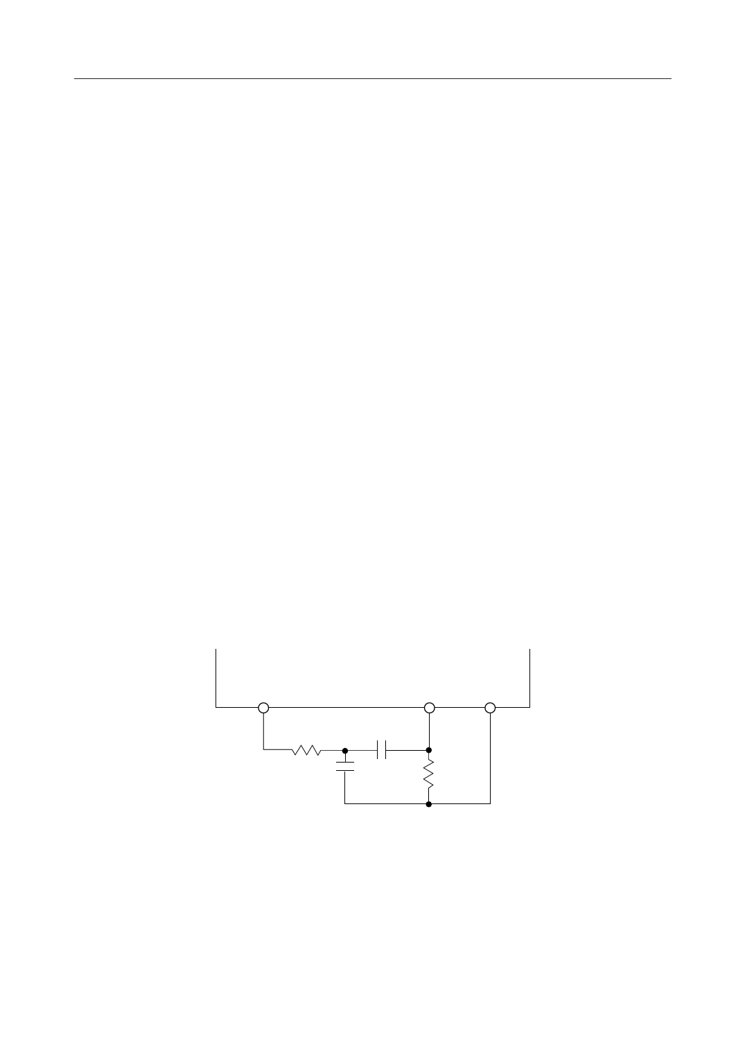
A circuit example for adjustment of frequency characteristics
TPAO
R3
TPBI
VSG
C3
R4
C4
TMX1I, TMX2I
Transmit addition signal inputs.
Through processor control, the input signals to TMX1I and TMX2I are added to the transmit
signal and are output to T1O and T2O respectively.
8/43
Share Link: 