MT90810 データシートの表示(PDF) - Mitel Networks
部品番号
コンポーネント説明
メーカー
MT90810 Datasheet PDF : 34 Pages
| |||
MT90810
Preliminary Information
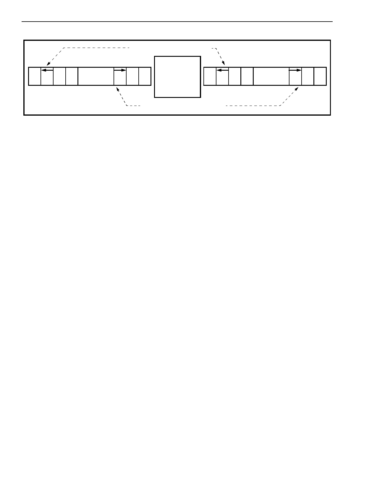
DC=0 for stream 0 channel 1
O/P
012
DSi0
I/P
.....
3
29 30 31
FMIC
I/P
DSo0 O/P
.....
0123
29 30 31
DC=1 for stream 0 channel 29
Figure 3 - Per-channel Direction Control
Connection Memory
Connection memory is comprised of a static RAM
block 384 locations by 12 bits. Each location in
connection memory corresponds to one of the 384
output channels. The mapping of memory location to
output channel is the same as the mapping of input
channel to data memory location and is shown in
Table 19 - “Connection Memory Mapping”.
The lower 8 bits of connection memory form
connection memory low byte as shown in Figure 10 -
“Connection Memory Low Byte”. The bits are defined
in Table 20, “Connection Memory Low Bits”.
The upper 4 bits of connection memory form
connection memory high (refer to Figure 11 -
“Connection memory high byte” ). Connection
memory low byte, together with the least significant
bit of connection memory high form an address to
point to in data memory. The location pointed to in
data memory provides the data for a given output
channel. The remaining three bits in connection
memory high are control bits. These bits perform
slightly different functions for MVIP and local
channels. The control bits in connection memory
high for MVIP streams enable/disable output drivers,
specify message or connection mode for individual
output channels, and determine the direction of the
DSi/DSo channel pair (see Table 21 - “Connection
Memory High Bits for MVIP channels” for further
details). The control bits in connection memory high
for local streams enable/disable DMA transfer,
specify message or connection mode for individual
output channels, and control CSTo timing (see Table
22 - “Connection Memory High Bits for Local
channels” for further details).
Connection memory can be read and written by the
microprocessor (see “Software Control” for further
details). When writing to connection memory, it is
necessary to first write the low bits and then the high
bits. The low bits are held in a temporary register
until the high bits are written. The complete write of
all 12 bits (to connection memory) is only performed
when the high bits are being written.
Connection and Message Modes
In connection mode, the connection memory low
byte and the least significant bit of connection
memory high form a 9 bit address to point to in data
memory. The location pointed to specifies which
source/input channel to connect to the respective
output channel and stream. The same source
channel can be routed to various output channels,
thus providing broadcast facility within the switch.
In message mode, the connection memory low byte
is sent directly out the corresponding output channel
and stream. The least significant bit of connection
memory high is not used.
Direction Control Bit
The direction control (DC) bit in connection memory
high determines the direction of the associated DSi-
DSo channel pair. If the DSi or DSo channel is
programmed as an input, the corresponding DSo or
DSi channel will automatically be configured as an
output. Thus, there are always 256 MVIP input and
256 MVIP output channels or 256 full duplex MVIP
channels on the MVIP bus. Figure 3 - “Per channel
direction control” illustrates the use of DC bit for
direction control on stream 0 channel 1 and channel
29. When DC bit is set, DSo channel is output from
the FMIC and DSi is input to the FMIC. When DC bit
is cleared, the channel directions are reversed.
Timing and Clock Control
The FMIC clock control circuitry contains an on-chip
analog PLL (with external loop filter) which is
designed to phase lock to a 4.096MHz clock. The on-
chip VCO runs at eight times this rate yielding a
32MHz clock which is divided by two. The resulting
16.384MHz is used as the internal master clock of
the FMIC.
The input to the analog PLL can be selected from
among several different sources including, the MVIP
C4 clock which is used as the internal master clock
of the FMIC.
The on-chip digital PLL generates a 4.096MHz clock
which is phase locked to an externally generated
2-150
Share Link: 