MT9300 データシートの表示(PDF) - Mitel Networks
部品番号
コンポーネント説明
メーカー
MT9300 Datasheet PDF : 29 Pages
| |||
MT9300
Advance Information
When Extended Delay or Back-to-Back
configuration is selected, Control Register A1/B1 and
Control Register 2 of the selected group of echo
cancellers require special care. Refer to the Register
description section.
Table 2 is a list of the channels used for the 16
groups of echo cancellers when they are configured
as Extended Delay or Back-to-Back
Normal Configuration
For a given group (group 0 to 15), 2 PCM I/O
channels are used. For example, group 1 Echo
Cancellers A and B, channels 2 and 3 are active.
Group Channel Group Channel
0
0, 1
8
16, 17
1
2, 3
9
18, 19
2
4, 5
10
20, 21
3
6, 7
11
22, 23
4
8, 9
12
24, 25
5
10, 11
13
26, 27
6
12, 13
14
28, 29
7
14, 15
15
30, 31
Table 2 - Group and Channel allocation
Extended Delay Configuration
For a given group (group 0 to 15), only one PCM I/O
channel is active (Echo Canceller A) and the other
channel carries don’t care data. For example, group
2, Echo Canceller A (Channel 4) will be active and
Echo Canceller B (Channel 5) will carry don’t care
data.
Back-to-Back Configuration
For a given group (group 0 to 15), only one PCM I/O
channel is active (Echo Canceller A) and the other
channel carries don’t care data. For example, group
5, Echo Canceller A (Channel 10) will be active and
Echo Canceller B (Channel 11) will carry don’t care
data.
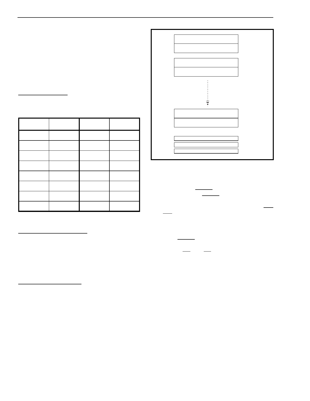
Group 0
Echo
Cancellers
Registers
Channel 0, EC A Ctrl/Stat Registers
Channel 1, EC B Ctrl/Stat Registers
0000h --> 001Fh
0020h --> 003Fh
Group 1
Echo
Cancellers
Registers
Channel 2, EC A Ctrl/Stat Registers
Channel 3, EC B Ctrl/Stat Registers
0040h --> 005Fh
0060h --> 007Fh
Groups 2 --> 14
Echo Cancellers
Registers
Group 15
Echo
Cancellers
Registers
Channel 30, EC A Ctrl/Stat Registers
Channel 31, EC B Ctrl/Stat Registers
03C0h --> 03DFh
03E0h --> 03FFh
Main Control Registers <15:0>
Interrupt FIFO Register
Test Register
0400h --> 040Fh
0410h
0411h
Figure 8 - Memory Mapping
Power Up Sequence
On power up, the RESET pin must be held low for
100µs. Forcing the RESET pin low will put the
MT9300 in power down state. In this state, all
internal clocks are halted, D<7:0>, Sout, Rout, DTA
and IRQ pins are tristated. The 16 Main Control
Registers, the Interrupt FIFO Register and the Test
Register are reset to zero.
When the RESET pin returns to logic high and a
valid MCLK is applied, the user must wait 500µs for
PLL to lock. C4i and F0i can be active during this
period. Once the PLL has locked, the user must
power up the 16 groups of echo cancellers
individually, by writing a “1” into the PWUP bit in
each group of echo canceller’s Main Control
Register.
For each group of echo cancellers, when the PWUP
bit toggles from zero to one, echo cancellers A and B
execute their initialization routine. The initialization
routine sets their registers, Base Address+00H to
Base Address+3FH, to the default Reset Value and
clears the Adaptive Filter coefficients. Two frames
are necessary for the initialization routine to execute
properly.
Once the initialization routine is executed, the user
can set the per channel Control Registers, Base
Address+00H to Base Address+3FH, for the specific
application.
10
Share Link: 