MTV048 データシートの表示(PDF) - Unspecified
部品番号
コンポーネント説明
メーカー
MTV048 Datasheet PDF : 19 Pages
| |||
MYSON
TECHNOLOGY
MTV048
(Rev 0.9)
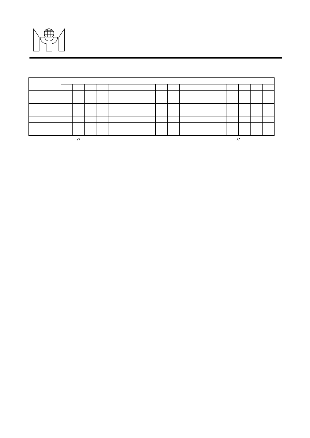
TABLE 3. Repeat Line Number of Character
Repeat Line
Repeat Line #
Weight 0 1 2 3 4 5 6 7 8 9 10 11 12 13 14 15 16 17
+1
- - - - - - - -v- - - - - - - - -
+2
- - - -v- - - - - - -v- - - - -
+4
- -v- - -v- - -v- - -v- - -
+8
-v-v-v-v-v-v-v-v- -
+16
- vvvvvvvvvvvvvvvv -
+17
vvvvvvvvvvvvvvvvv -
+18
vvvvvvvvvvvvvvvvvv
Note: “v” means the nth line in the character would be repeated once, while “-“ means the nth line in the
character would not be repeated.
3.4 Horizontal Display Control
The horizontal display control is used to generate control timing for horizontal display based on double char-
acter width bit (CWS), horizontal positioning register (HORD), horizontal resolution register (HORR), and
HFLB input. A horizontal display line consists of (HORR*12) dots which include 360 dots for 30 display char-
acters and the remaining dots for blank region. The horizontal delay starting from HFLB leading edge is
calculated by using the following equation:
For CRT: Horizontal delay time = ( HORD * 6 + 49) * P - phase error detection pulse width
Where P = One pixel display time = One horizontal line display time / (HORR*12)
For LCD: Horizontal delay time = ( HORD * 6 + 49) * P
Where P = One XIN pixel display time
3.5 Phase lock loop (PLL)
On-chip PLL generates system clock timing (VCLK) by tracking the input HFLB and horizontal resolution reg-
ister (HORR). The frequency of VCLK is determined by the following equation:
VCLK Freq. = HFLB Freq. * HORR * 12
The VCLK frequency ranges from 6MHz to 150MHz selected by (VCO1, VCO0). In addition, when HFLB
input is not present to MTV048, the PLL will generate a specific system clock, approximately 2.5MHz, by a
built-in oscillator to ensure data integrity.
3.6 Display & Row Control Registers
The internal RAM contains display and row control registers. The display registers have 450 locations, which
are allocated between (row 0, column 0) to (row 14, column 29), as shown in Figure 4. Each display register
has its corresponding character address on ADDRESS byte, its corresponding background color, 1 blink bit
and its corresponding color bits on ATTRIBUTE bytes. The row control register is allocated at column 30 for
row 0 to row 14, it is used to set character size to each respective row. If double width character is chosen,
only even column characters could be displayed on screen and the odd column characters will be hidden.
Rev 0.9
-6-
2001/03/15
Share Link: 