CY7C4201(2010) データシートの表示(PDF) - Cypress Semiconductor
部品番号
コンポーネント説明
メーカー
CY7C4201 Datasheet PDF : 20 Pages
| |||
CY7C4421/4201/4211/4221
CY7C4231/4241/4251
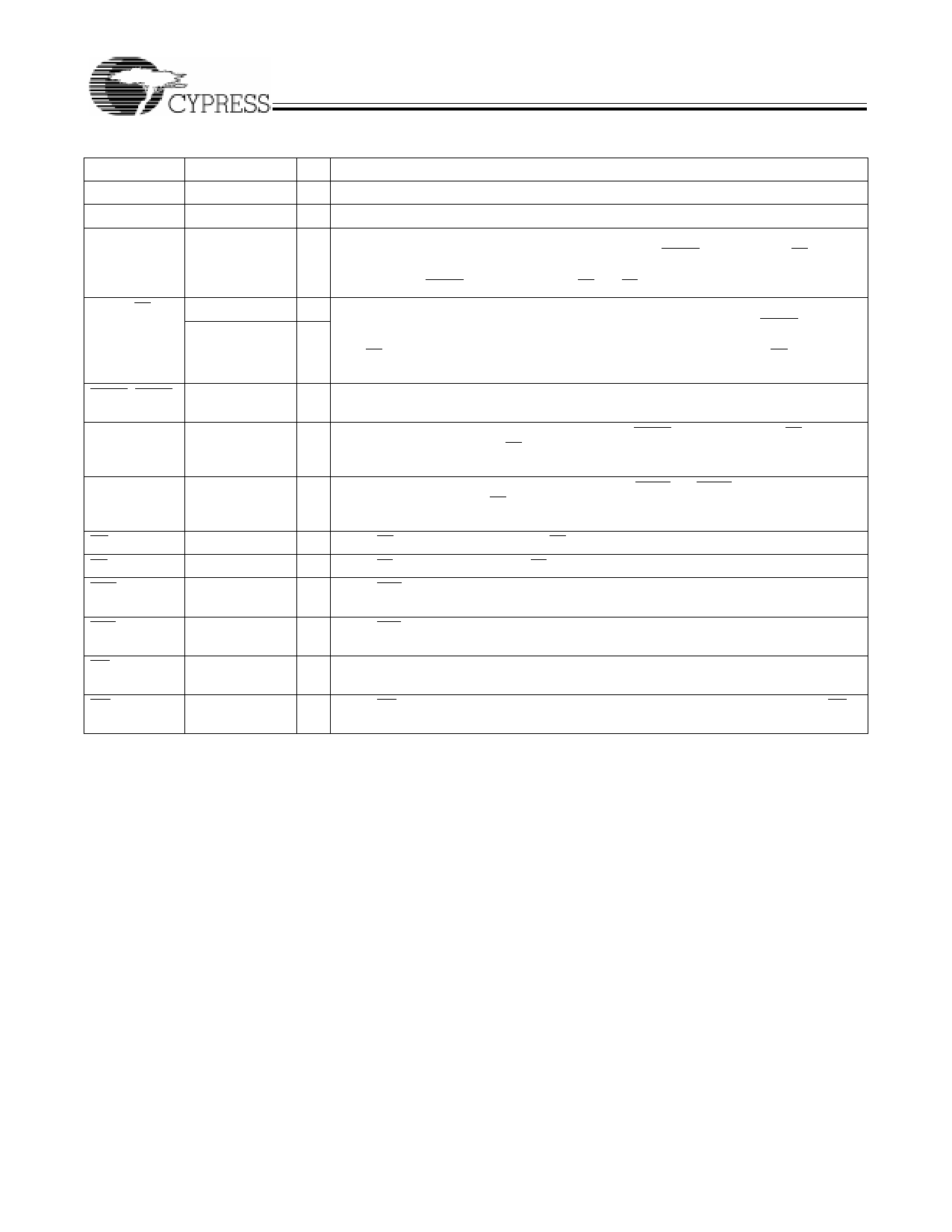
Selection Guide
Description
-10
-15
Maximum Frequency
100
66.7
Maximum Access Time
8
10
Minimum Cycle Time
10
15
Minimum Data or Enable Setup
3
4
Minimum Data or Enable Hold
0.5
1
Maximum Flag Delay
8
10
Active Power Supply Current
Commercial
35
35
Industrial
40
40
Density
CY7C4421
64 × 9
Pin Configuration
CY7C4201
256 × 9
PLCC
Top View
CY7C4211
512 × 9
CY7C4221
1K × 9
CY7C4231
2K × 9
Figure 1. Pin Diagram
TQFP
Top View
-25
40
15
25
6
1
15
35
40
CY7C4241
4K × 9
Unit
MHz
ns
ns
ns
ns
ns
ICC1
CY7C4251
8K × 9
D1
D0
PAF
PAE
GND
REN1
RCLK
REN2
OE
4 3 2 1 32 3130
5
29
6
28
7
27
8
26
9
25
10
24
11
23
12
22
13
21
14 1516 17 1819 20
RS
WEN1
WCLK
WEN2/LD
VCC
Q8
Q7
Q6
Q5
D1
D0
PAF
PAE
GND
REN1
RCLK
REN2
32 31 30 29 28 27 26 25
1
24
2
23
3
22
4
21
5
20
6
19
7
18
8
17
9 10 11 12 13 14 15 16
WEN1
WCLK
WEN2/LD
VCC
Q8
Q7
Q6
Q5
Table 1. Pin Definitions
Pin
D0–8
Q0–8
WEN1
Name
Data Inputs
Data Outputs
Write Enable 1
WEN2/LD Dual Write Enable 2
Mode Pin
Load
REN1, REN2
WCLK
Read Enable
Inputs
Write Clock
I/O
Description
I Data inputs for 9-bit bus.
O Data outputs for 9-bit bus.
I The only write enable to have programmable flags when device is configured. Data is
written on a LOW-to-HIGH transition of WCLK when WEN1 is asserted and FF is HIGH.
If the FIFO is configured to have two write enables, data is written on a LOW-to-HIGH
transition of WCLK when WEN1 is LOW and WEN2/LD and FF are HIGH.
I If HIGH at reset, this pin operates as a second write enable. If LOW at reset, this pin
I
operates as a control to write or read the programmable flag offsets. WEN1 must be
LOW and WEN2 must be HIGH to write data into the FIFO. Data is not written into the
FIFO if the FF is LOW. If the FIFO is configured to have programmable flags, WEN2/LD
is held LOW to write or read the programmable flag offsets.
I Enables device for read operation.
I The rising edge clocks data into the FIFO when WEN1 is LOW, WEN2/LD is HIGH, and
the FIFO is not Full. When LD is asserted, WCLK writes data into the programmable
flag-offset register.
Document #: 38-06016 Rev. *D
Page 3 of 20
[+] Feedback
Share Link: 