CY7C4231-25JC データシートの表示(PDF) - Cypress Semiconductor
部品番号
コンポーネント説明
メーカー
CY7C4231-25JC Datasheet PDF : 21 Pages
| |||
CY7C4421/4201/4211/4221
CY7C4231/4241/4251
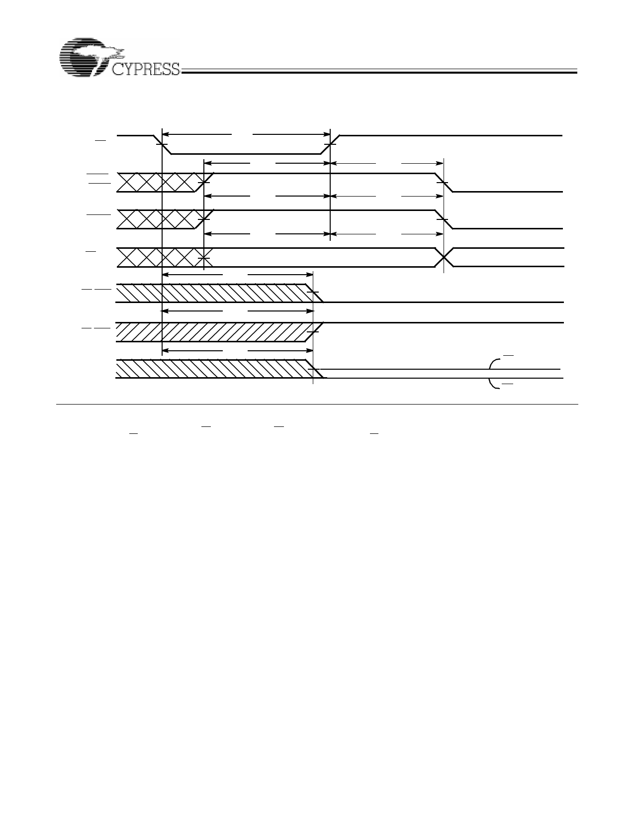
Switching Waveforms (continued)
Reset Timing[13]
RS
REN1,
REN2
WEN1
WEN2/LD [15]
EF,PAE
FF,PAF,
Q0 - Q8
tRS
tRSS
tRSS
tRSS
tRSF
tRSF
tRSF
tRSR
tRSR
tRSR
OE=1 [14]
OE=0
42X1–8
Notes:
13. The clocks (RCLK, WCLK) can be free-running during reset.
14. After reset, the outputs will be LOW if OE = 0 and three-state if OE=1.
15. Holding WEN2/LD HIGH during reset will make the pin act as a second enable pin. Holding WEN2/LD LOW during reset will make the pin act as a load enable for the
programmable flag offset registers.
7
Share Link: 