NAND01G-A データシートの表示(PDF) - STMicroelectronics
部品番号
コンポーネント説明
メーカー
NAND01G-A
STMicroelectronics

NAND01G-A Datasheet PDF : 57 Pages
| |||
NAND128-A, NAND256-A
NAND512-A, NAND01G-A
128 Mbit, 256 Mbit, 512 Mbit, 1 Gbit (x8/x16)
528 Byte/264 Word Page, 1.8V/3V, NAND Flash Memories
FEATURES SUMMARY
■ HIGH DENSITY NAND FLASH MEMORIES
– Up to 1 Gbit memory array
– Up to 32 Mbit spare area
– Cost effective solutions for mass storage
applications
■ NAND INTERFACE
– x8 or x16 bus width
– Multiplexed Address/ Data
– Pinout compatibility for all densities
■ SUPPLY VOLTAGE
– 1.8V device: VDD = 1.7 to 1.95V
– 3.0V device: VDD = 2.7 to 3.6V
■ PAGE SIZE
– x8 device: (512 + 16 spare) Bytes
– x16 device: (256 + 8 spare) Words
■ BLOCK SIZE
– x8 device: (16K + 512 spare) Bytes
– x16 device: (8K + 256 spare) Words
■ PAGE READ / PROGRAM
– Random access: 12µs (max)
– Sequential access: 50ns (min)
– Page program time: 200µs (typ)
■ COPY BACK PROGRAM MODE
– Fast page copy without external buffering
■ FAST BLOCK ERASE
– Block erase time: 2ms (Typ)
■ STATUS REGISTER
■ ELECTRONIC SIGNATURE
■ CHIP ENABLE ‘DON’T CARE’ OPTION
– Simple interface with microcontroller
■ SERIAL NUMBER OPTION
■ HARDWARE DATA PROTECTION
– Program/Erase locked during Power
transitions
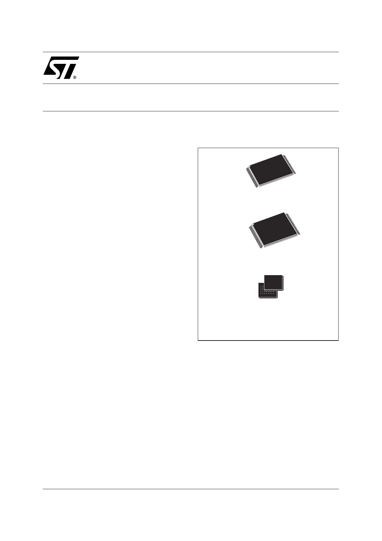
Figure 1. Packages
TSOP48 12 x 20mm
USOP48 12 x 17 x 0.65mm
FBGA
VFBGA55 8 x 10 x 1mm
TFBGA55 8 x 10 x 1.2mm
VFBGA63 9 x 11 x 1mm
TFBGA63 9 x 11 x 1.2mm
■ DATA INTEGRITY
– 100,000 Program/Erase cycles
– 10 years Data Retention
■ RoHS COMPLIANCE
– Lead-Free Components are Compliant
with the RoHS Directive
■ DEVELOPMENT TOOLS
– Error Correction Code software and
hardware models
– Bad Blocks Management and Wear
Leveling algorithms
– File System OS Native reference software
– Hardware simulation models
February 2005
1/57
Share Link: