NB100LVEP221(2003) データシートの表示(PDF) - ON Semiconductor
部品番号
コンポーネント説明
メーカー
NB100LVEP221 Datasheet PDF : 10 Pages
| |||
NB100LVEP221
VCC0
Q5
Q5
Q4
Q4
Q3
Q3
Q2
Q2
Q1
Q1
Q0
Q0
39 38 37 36 35 34 33 32 31 30 29 28 27
40
26
41
25
42
24
43
23
44
22
45
21
46
NB100LVEP221
20
47
19
48
18
49
17
50
16
51
15
52
14
1 2 3 4 5 6 7 8 9 10 11 12 13
Q12
Q12
Q13
Q13
Q14
Q14
Q15
Q15
Q16
Q16
Q17
Q17
VCC0
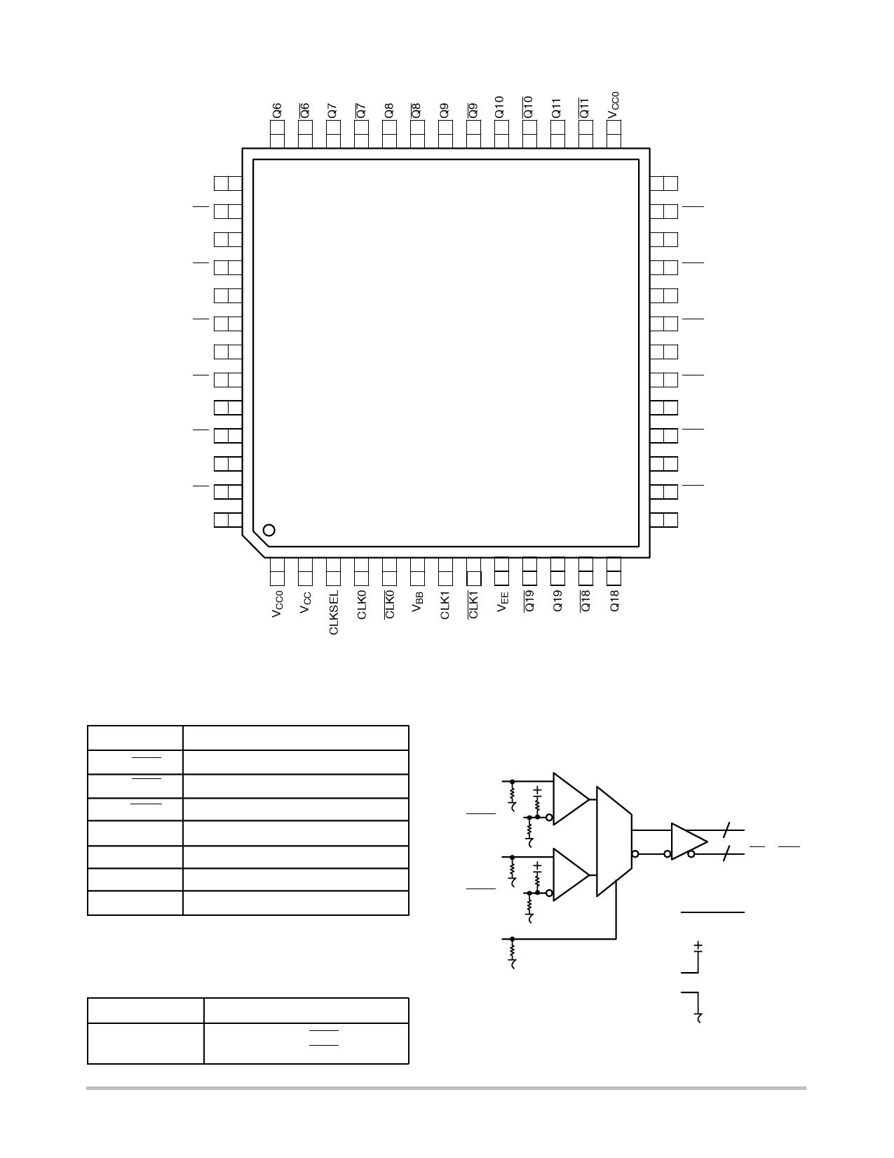
All VCC, VCCO, and VEE pins must be externally connected to appropriate Power Supply to guarantee proper operation. The thermally
conductive exposed pad on package bottom (see package case drawing) must be attached to a heat-sinking conduit, capable of transfer-
ring 1.2 Watts. This exposed pad is electrically connected to VEE internally.
Figure 1. 52-Lead LQFP Pinout (Top View)
PIN DESCRIPTION
PIN
CLK0*, CLK0**
CLK1*, CLK1**
Q0:19, Q0:19
CLK_SEL*
VBB
FUNCTION
ECL/PECL Differential Inputs
ECL/PECL or HSTL Differential Inputs
ECL/PECL Differential Outputs
ECL/PECL Active Clock Select Input
Reference Voltage Output
VCC/VCCO
Positive Supply
VEE***
Negative Supply
* Pins will default LOW when left open.
** Pins will default HIGH when left open.
*** The thermally conductive exposed pad on the bottom of the
package is electrically connected to VEE internally.
FUNCTION TABLE
CLK_SEL
Active Input
L
CLK0, CLK0
H
CLK1, CLK1
CLK0
CLK0
CLK1
CLK1
CLK_SEL
0
1
VBB
VCC
VEE
Figure 2. Logic Diagram
20
Q0 - Q19
Q0 - Q19
20
http://onsemi.com
2
Share Link: 