NCP1075 データシートの表示(PDF) - ON Semiconductor
部品番号
コンポーネント説明
メーカー
NCP1075 Datasheet PDF : 30 Pages
| |||
NCP1070, NCP1071, NCP1072, NCP1075, NCP1076, NCP1077
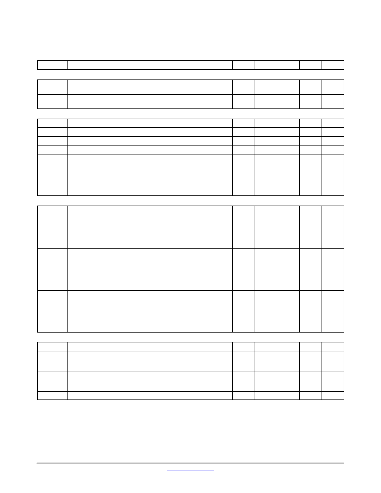
ELECTRICAL CHARACTERISTICS
(For all NCP107X products except NCP1072P100BG: For typical values TJ = 25°C, for min/max values TJ = −40°C to +125°C, VCC = 8 V
unless otherwise noted)
(For NCP1072P100BG: For typical values TJ = 25°C, for min/max values TJ = −55°C (Note 7) to +125°C, VCC = 8 V unless otherwise noted)
Symbol
Rating
Pin
Min
Typ
Max
Unit
FEEDBACK SECTION
VFB(REF) Equivalent pull−up voltage in linear regulation range
(Guaranteed by design)
4
3.3
V
RFB(up) Equivalent feedback resistor in linear regulation range
(Guaranteed by design)
4
19.5
kW
FREQUENCY FOLDBACK & SKIP
IFBfold
IFBfold(end)
Fmin
IFBskip
IFreeze
Start of frequency foldback feedback level
End of frequency foldback feedback level, Fsw = Fmin
The frequency below which skip−cycle occurs
The feedback level to enter skip mode
Internal minimum current setpoint (IFB = IFBFreeze)
NCP1070
NCP1071
NCP1072
NCP1075
NCP1076
NCP1077
4
−
−68
−
mA
4
−
−100
−
mA
−
21
25
29
kHz
4
−
−120
−
mA
mA
−
−
88
−
−
123
−
−
88
−
−
168
−
−
228
−
−
280
−
RAMP COMPENSATION
Sa(65)
The internal ramp compensation @ 65 kHz
NCP1070
NCP1071
NCP1072
NCP1075
NCP1076
NCP1077
mA/ms
−
−
7
−
−
10
−
−
4.2
−
−
7.5
−
−
15
−
−
18
−
Sa(100)
The internal ramp compensation @ 100 kHz
NCP1070
NCP1071
NCP1072
NCP1075
NCP1076
NCP1077
mA/ms
−
−
11
−
−
15
−
−
6.5
−
−
11.5
−
−
23
−
−
28
−
Sa(130)
The internal ramp compensation @ 130 kHz
NCP1070
NCP1071
NCP1072 (Note 5)
NCP1075
NCP1076
NCP1077
−
−
14
−
−
20
−
−
8.4
−
−
15
−
−
30
−
−
36
−
PROTECTIONS
tSCP
trecovery
Fault validation further to error flag assertion
OFF phase in fault mode
NCP1070/1/2/5/6/7
NCP1072P100BG
−
40
53
−
ms
ms
−
−
420
−
−
−
210
−
IOVP
VCC clamp current at which the switcher stops pulsing
NCP1070/71
NCP1072/75/76/77
mA
1
6.2
8.7
11.2
6
8.5
11
tOVP
The filter of VCC OVP comparator
−
−
80
−
ms
Product parametric performance is indicated in the Electrical Characteristics for the listed test conditions, unless otherwise noted. Product
performance may not be indicated by the Electrical Characteristics if operated under different conditions.
4. The final switch current is: IIPK(0) / (Vin/LP + Sa) x Vin/LP + Vin/LP x tprop, with Sa the built−in slope compensation, Vin the input voltage, LP
the primary inductor in a flyback, and tprop the propagation delay.
5. NCP1072 130 kHz on demand only.
6. Oscillator frequency is measured with disabled jittering.
7. For coldest temperature, QA sampling at −40°C in production and −55°C specification is Guaranteed by Characterization.
www.onsemi.com
7
Share Link: 