1207 データシートの表示(PDF) - ON Semiconductor
部品番号
コンポーネント説明
メーカー
1207 Datasheet PDF : 18 Pages
| |||
NCP1207
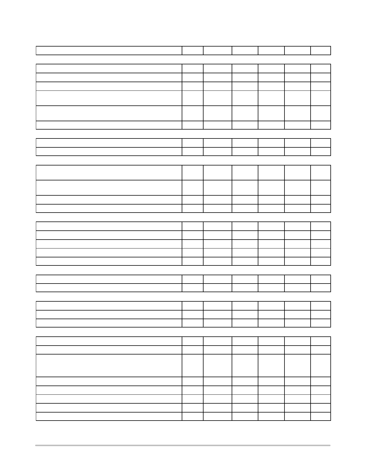
ELECTRICAL CHARACTERISTICS (For typical values TJ = 25°C, for min/max values TJ = 0°C to +125°C, Max TJ = 150°C,
VCC = 11 V unless otherwise noted)
Rating
Pin
Symbol
Min
Typ
Max
Unit
DYNAMIC SELF−SUPPLY
VCC Increasing Level at which the Current Source Turns−off
VCC Decreasing Level at which the Current Source Turns−on
VCC Decreasing Level at which the Latchoff Phase Ends
Internal IC Consumption, No Output Load on Pin 5,
FSW = 60 kHz
Internal IC Consumption, 1.0 nF Output Load on Pin 5,
FSW = 60 kHz
Internal IC Consumption in Latchoff Phase
INTERNAL STARTUP CURRENT SOURCE (TJ u 0°C)
High−voltage Current Source, VCC = 10 V
High−voltage Current Source, VCC = 0
DRIVE OUTPUT
6
VCCOFF
10.8
6
VCCON
9.1
6
VCClatch
−
6
ICC1
−
6
ICC2
−
6
ICC3
−
8
IC1
4.3
8
IC2
−
12
12.9
V
10
10.6
V
5.3
−
V
1.0
1.3
mA
(Note 1)
1.6
2.0
mA
(Note 1)
330
−
mA
7.0
9.6
mA
8.0
−
mA
Output Voltage Rise−time @ CL = 1.0 nF, 10−90% of Output
Signal
5
Tr
−
40
−
ns
Output Voltage Fall−time @ CL = 1.0 nF, 10−90% of Output
Signal
5
Tf
−
20
−
ns
Source Resistance
Sink Resistance
CURRENT COMPARATOR (Pin 5 Unloaded)
5
ROH
12
20
36
W
5
ROL
5.0
10
19
W
Input Bias Current @ 1.0 V Input Level on Pin 3
Maximum Internal Current Setpoint
Propagation Delay from Current Detection to Gate OFF State
Leading Edge Blanking Duration
Internal Current Offset Injected on the CS Pin during OFF Time
OVERVOLTAGE SECTION (VCC = 11 V)
Sampling Delay after ON Time
OVP Internal Reference Level
FEEDBACK SECTION (VCC = 11 V, Pin 5 Loaded by 1.0 kW)
Internal Pullup Resistor
3
IIB
−
3
ILimit
0.92
3
TDEL
−
3
TLEB
−
3
Iskip
−
1
Tsample
−
1
Vref
6.4
2
Rup
−
0.02
1.0
100
380
200
4.5
7.2
20
−
mA
1.12
V
160
ns
−
ns
−
mA
−
ms
8.0
V
−
kW
Pin 3 to Current Setpoint Division Ratio
−
Iratio
−
3.3
−
−
Internal Soft−Start
−
Tss
−
1.0
−
ms
DEMAGNETIZATION DETECTION BLOCK
Input Threshold Voltage (Vpin1 Decreasing)
Hysteresis (Vpin1 Decreasing)
Input Clamp Voltage
High State (Ipin 1 = 3.0 mA)
Low State (Ipin 1 = −2.0 mA)
Demag Propagation Delay
Internal Input Capacitance at Vpin1 = 1.0 V
Minimum TOFF (Internal Blanking Delay after TON)
Timeout After Last Demag Transition
Pin 1 Internal Impedance
1. Max value at TJ = 0°C.
1
VTH
35
50
90
mV
1
VH
−
20
−
mV
1
VCH
8.0
10
12
V
1
VCL
−0.9
−0.7
−0.5
V
1
Tdem
−
210
−
ns
1
Cpar
−
10
−
pF
1
Tblank
−
8.0
−
ms
1
Tout
−
5.0
−
ms
1
Rint
−
28
−
kW
http://onsemi.com
4
Share Link: 