NCP5603MNR2 データシートの表示(PDF) - ON Semiconductor
部品番号
コンポーネント説明
メーカー
NCP5603MNR2 Datasheet PDF : 13 Pages
| |||
NCP5603
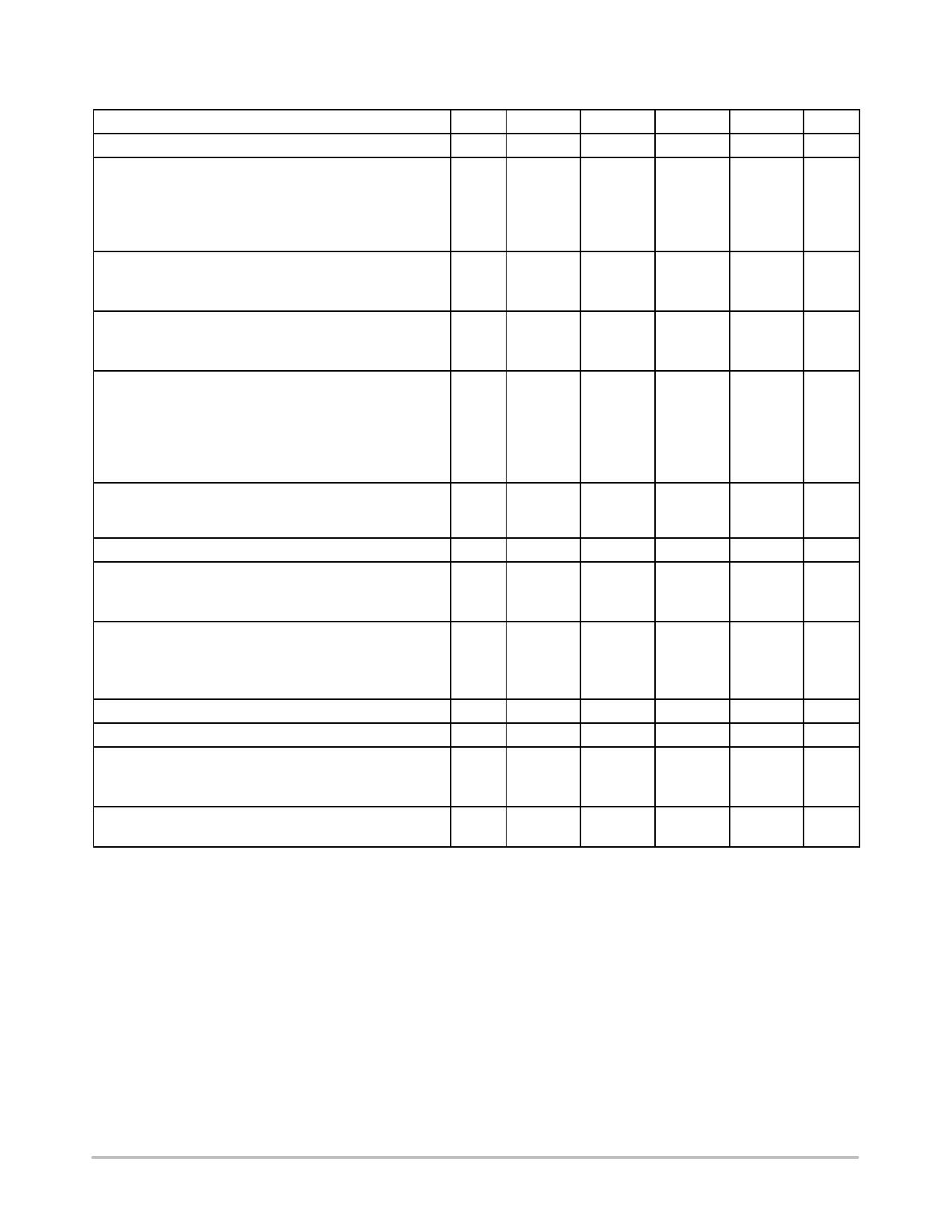
ELECTRICAL CHARACTERISTICS @ 2.85 V < Vbat < 5.5 V (−40°C to +85°C ambient temperature, unless otherwise noted).
Characteristic
Pin
Symbol
Min
Typ
Max
Unit
Power Supply
Quiescent Current @ Vbat = 3.7 V, Iout = 0 mA
@ Pulsed Clock Fop = 262 kHz
@ Pulsed Clock Fop = 650 kHz
@ Continuous Clock Fop = 262 kHz
@ Continuous Clock Fop = 650 kHz
3
Vbat
2.85
−
3
Iqsc
−
−
−
−
−
1.0
−
2.1
5.5
V
mA
0.8
1.2
−
−
Shutdown Current @ Iout = 0 mA, EN/PWM = L
@ 2.85 < Vbat < 4.2 V
@ Vbat = 5.5 V
Output Voltage Regulation
@ Vsel = 1, 2.85 V < Vbat < 4.5 V
@ Vsel = 0, 2.85 V < Vbat < 4.5 V
Continuous DC Load Current (Note 7)
Cin = 1.0 mF, CFLY = 1.0 mF, Cout = 1.0 mF
@ Vsel = 1, 3.2 V < Vbat < 4.5 V
@ Vsel = 0, 3.2 V < Vbat < 5.5 V
@ Vsel = 1, 2.85 V < Vbat < 4.5 V
@ Vsel = 0, 2.85 V < Vbat < 5.5 V
Pulsed Output Current
Cin = 10 mF, CFLY = 1.0 mF, Cout = 10 mF, Vbat = 3.6 V
Pwidth = 500 ms, −40°C < TA < +65°C
Output Continuous Short Circuit Current, Vout = 0 V
Operating Frequency (Note 5)
@ Fsel = 0, 2.85 V < Vbat < 4.5 V
@ Fsel = 1, 2.85 V < Vbat < 4.5 V
3
Istdb
−
−
mA
−
2.5
−
4.0
3
Vout
V
4.75
5.0
5.25
4.275
4.5
4.725
3
Iout
mA
−
−
−
−
3
IFLH
−
160
−
200
−
80
−
120
mA
−
350
−
3
Isch
−
40
100
mA
Fop
kHz
210
262
320
500
650
1000
Output Voltage Ripple (Note 6)
Fop = 262 kHz, Iout = 60 mA (Note 7)
@ Cout = 1.0 mF
@ Cout = 4.7 mF
3
VPP
mV
−
150
−
−
25
60
Digital Input High Level
4, 5, 6
VIH
1.3
−
−
V
Digital Input Low level
4, 5, 6
VIL
−
−
0.4
V
Output Power Efficiency
@ Vbat = 3.3 V, Vout = 5.0 V, Iout = 60 mA, Fop = 262 kHz
@ Vbat = 3.9 V, Vout = 5.0 V, Iout = 160 mA, Fop = 650 kHz
Ph
%
−
75
−
−
84
−
Thermal Shut Down Protection
Hysteresis
THSD
−
160
−
°C
−
20
−
5. Temperature range guaranteed by design, not production tested.
6. Smaller footprint associated to lower working voltages (10 V or 6.3 V, size 0805 or 0602) can be used, but care must be observed to prevent
DC bias effect on the capacitance final value. See capacitor manufacturer data sheets.
7. Ceramic X7R, ESR < 100 mW, SMD type capacitors are mandatory to achieve the Iout specifications. Depending upon the PCB layout, it
might be necessary to use two 2.2 mF/6.3 V/ceramic capacitors in parallel, yielding an improved Vout noise over the temperature range. On
the other hand, care must be observed to take into account the DC bias impact on the capacitance value. See ceramic capacitor manufacturer
data sheets.
8. Digital inputs undershoot < − 0.30 V to ground, Digital inputs overshoot < 0.30 V to Vbat.
http://onsemi.com
6
Share Link: 