AD9802 データシートの表示(PDF) - Analog Devices
部品番号
コンポーネント説明
メーカー
AD9802 Datasheet PDF : 20 Pages
| |||
AD9802
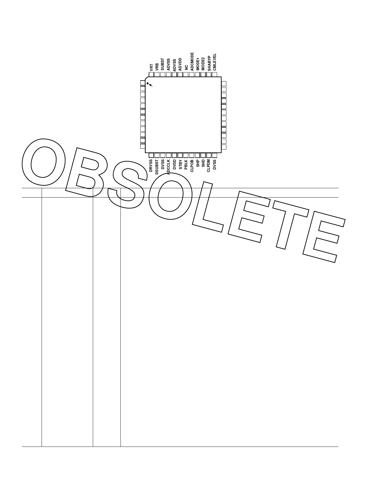
PIN CONFIGURATION
48 47 46 45 44 43 42 41 40 39 38 37
ADVSS 1
(LSB) D0 2
PIN 1
IDENTIFIER
36 ADCIN
35 TEST2
D1 3
34 TEST1
D2 4
33 ACVDD
D3 5
D4 6
D5 7
D6 8
AD9802
TOP VIEW
(Not to Scale)
32 CLAMP_BIAS
31 ACVSS
30 PGACONT2
29 PGACONT1
D7 9
28 CCDBYP1
OBSOLETE Pin #
1
2–11
12
13
14
15
16
Pin Name
ADVSS
D0–D9
DRVDD
DRVSS
DSUBST
DVSS
ADCCLK
D8 10
(MSB) D9 11
DRVDD 12
27 PIN
26 DIN
25 CCDBYP2
NC = NO CONNECT 13 14 15 16 17 18 19 20 21 22 23 24
Type
P
DO
P
P
P
P
DI
PIN FUNCTION DESCRIPTIONS
Description
Analog Ground
Digital Data Outputs: D0 = LSB, D9 = MSB
+3 V Digital Driver Supply
Digital Driver Ground
Digital Substrate
Digital Ground
ADC Sample Clock Input
17
DVDD
P
+3 V Digital Supply
18
STBY
DI
Power-Down (Active High)
19
PBLK
DI
Pixel Blanking (Active Low)
20
CLPOB
DI
Black Level Restore Clamp (Active Low)
21
SHP
DI
Reference Sample Clock Input
22
SHD
DI
Data Sample Clock Input
23
CLPDM
DI
Input Clamp (Active Low)
24
DVSS
P
Digital Ground
25
CCDBYP2
AO
CCD Bypass. Decouple to analog ground through 0.1 µF.
26
DIN
AI
CDS Input. Tie to Pin 27 and AC-Couple to CCD output through 0.1 µF.
27
PIN
AI
CDS Input. See above.
28
CCDBYP1
AO
CCD Bypass. Decouple to analog ground through 0.1 µF.
29
PGACONT1
AI
Coarse PGA Gain Control (0.3 V–2.7 V). Decoupled to analog ground through 0.1 µF.
30
PGACONT2
AI
Fine PGA Gain Control
31
ACVSS
P
Analog Ground
32
CLAMP_BIAS AO
Clamp Bias Level. Decouple to analog ground through 0.1 µF.
33
ACVDD
P
+3 V Analog Supply
34, 35 TEST1, TEST2 AI
Reserved Test Pins. Should be left NC or pulled high to ACVDD.
36
ADCIN
AI
Direct ADC Analog Input (See Driving the Direct ADC Input)
37
CMLEVEL
AO
Common-Mode Level. Decouple to analog ground through 0.1 µF.
38
SHABYP
AO
Internal Bias Level. Decouple to analog ground through 0.1 µF.
39
MODE2
DI
ADC Test Mode Control (See Digital Output Data Control.)
40
MODE1
DI
ADC Test Mode Control (See Digital Output Data Control.)
41
ADCMODE
DI
ADC Input Control. Logic low for CDS/PGA, high for direct input.
42
NC
No Connect
43
ADVDD
P
+3 V Analog Supply
44, 45 ADVSS
P
Analog Ground
46
SUBST
P
Substrate. Connect to analog ground.
47
VRB
AO
Bottom Reference Bypass. Decouple to analog ground through 0.1 µF.
48
VRT
AO
Top Reference Bypass
NOTE
Type: AI = Analog Input, AO = Analog Output, DI = Digital Input, DO = Digital Output, P = Power.
–4–
REV. 0
Share Link: 