AD9802 データシートの表示(PDF) - Analog Devices
部品番号
コンポーネント説明
メーカー
AD9802 Datasheet PDF : 20 Pages
| |||
AD9802
THEORY OF OPERATION
Introduction
The AD9802 is a 10-bit analog-to-digital interface for CCD
cameras. The block level diagram of the system is shown in
Figure 14. The device includes a correlated double sampler
(CDS), 0 dB–31 dB variable gain amplifier (PGA), black level
correction loop, input clamp and voltage reference. The only
external analog circuitry required at the system level is an emit-
ter follower buffer between the CCD output and AD9802
inputs.
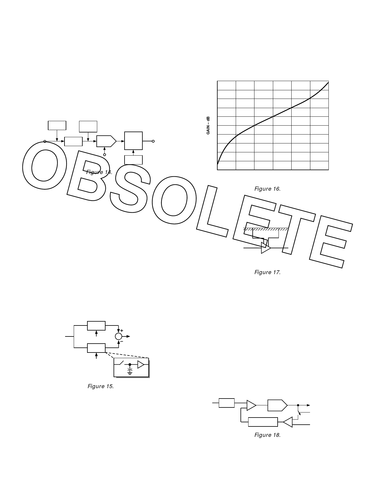
Programmable Gain Amplifier (PGA)
The on-chip PGA provides a (linear in dB) gain range of 0 dB–
31.5 dB. A typical gain characteristic plot is shown in Figure 16.
Only the range from 0.3 V to 2.7 V is intended for actual use.
35
30
25
20
15
CLAMP
BLACK
10
LEVEL
5
OBSOLETE 10-BIT
IN
CDS
PGA
ADC
OUT
GAIN
REF
Figure 14.
Correlated Double Sampling (CDS)
CDS is important in high performance CCD systems as a method
for removing several types of noise. Basically, two samples of the
CCD output are taken: one with the signal present (data) and one
without (reference). Subtracting these two samples removes
any noise that is common to—or correlates with—both.
Figure 15 shows the block diagram of the AD9802’s CDS. The
S/H blocks are directly driven by the input and the sampling
function is performed passively, without the use of amplifiers.
This implementation relies on the off-chip emitter follower
buffer to drive the two 10 pF sampling capacitors. Only one
0
–5
–10
–15
0
0.5
1
1.5
2
2.5
3
PGACONT1 – Volts
Figure 16.
As shown in Figure 17, PGA control is provided through the
PGACONT1 and PGACONT2 inputs. PGACONT1 provides
coarse, and PGACONT2 fine (1/16), gain control.
PGACONT1 PGACONT2
A
capacitor at a time is seen at the input pin.
PGACONT1 = COARSE CONTROL
PGACONT2 = FINE (1/16) CONTROL
The AD9802 actually uses two CDS circuits in a “ping-pong”
fashion to allow the system more acquisition time. In this way,
Figure 17.
the output from one of the two CDS blocks will be valid for an Black Level Clamping
entire clock cycle. Thus, the bandwidth requirement of the
For correct processing, the CCD signal must be referenced to a
subsequent gain stage is reduced as compared to that for a
well established “black level” by the AD9802. At the edge of the
single CDS channel system. This lower bandwidth translates to CCD, there is a collection of pixels covered with metal to pre-
lower power and noise.
vent any light penetration. As the CCD is read out, these “black
pixels” provide a calibration signal that is used to establish the
black level.
S/H
FROM
CCD
Q1
S
OUT
The feedback loop shown in Figure 18 is closed around the
PGA during the calibration interval (CLPOB = LOW) to set the
S/H
black level. As the black pixels are being processed, an integra-
tor block measures the difference between the input level and
Q2
10pF
the desired reference level. This difference, or error, signal is
amplified and passed to the CDS block where it is added to the
incoming pixel data. As a result of this process, the black pixels
are digitized at one end of the ADC range, taking maximum
Figure 15.
advantage of the available linear range of the system.
IN
CDS
PGA
INTEGRATOR
Figure 18.
ADC
CLPOB
NEG REF
–8–
REV. 0
Share Link: 