NCV7382 データシートの表示(PDF) - ON Semiconductor
部品番号
コンポーネント説明
メーカー
NCV7382 Datasheet PDF : 16 Pages
| |||
NCV7382
System designs can have an external resistor (1 k) in
series with an external diode to the battery, but short circuit
current from bus to ground can be reduced dramatically by
using the INH pin as termination pin for the master pullup
(See Figure 10 − Application Circuitry).
With this new setup, the controller can detect a short
circuit of the bus to ground (RxD timeout) and the
transceiver can be set into sleep mode. The INH pin will be
floating in this case, and the external master pullup resistor
will be disconnected from the bus line. Additionally, the
internal slave termination resistor is switched off and only
a high impedance termination is applied to the bus (typ.
75 mA). This will reduce the failure current of the system
by at least an order of magnitude, preventing a fast
Application Hints
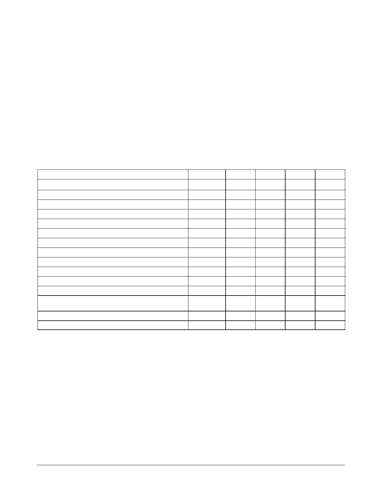
LIN System Parameter
Bus Loading Requirements
Parameter
Operating Voltage Range
Voltage Drop of Reverse Protection Diode
Voltage Drop at the Serial Diode in Pullup Path
Battery Shift Voltage
Ground Shift Voltage
Master Termination Resistor
Slave Termination Resistor
Number of System Nodes
Total Length of Bus Line
Line Capacitance
Capacitance of Master Node
Capacitance of Slave Node
Total Capacitance of the Bus including Slave and Master
Capacitance
Network Total Resistance
Time Constant of Overall System
discharge of the car battery. If the failure is removed, the
bus level will become recessive again and will wakeup the
system even if no local wakeup is present or possible.
Thermal Overload
The NCV7382 is protected against thermal overloads. If
the chip temperature exceeds the thermal shutdown
threshold, the transmitter is switched off until thermal
recovery. The receiver continues to work during thermal
shutdown.
Undervoltage VCC
The VCC undervoltage lockout feature disables the
transmitter until it is above the undervoltage lockout
threshold to prevent undesirable bus traffic.
Symbol
Min
VBAT
8.0
VDrop_rev
0.4
VSerDiode
0.4
VShift_BAT
0
VShift_GND
0
Rmaster
900
Rslave
20
N
2.0
LENBUS
−
CLINE
−
CMaster
−
CSlave
−
CBUS
1.0
RNetwork
537
t
1.0
Typ
−
0.7
0.7
−
−
1000
30
−
−
100
220
220
4.0
−
−
Max
18
1.0
1.0
0.1
0.1
1100
60
16
40
150
−
250
10
863
5.0
Unit
V
V
V
VBAT
VBAT
W
kW
−
m
pF/m
pF
pF
nF
W
ms
Recommendations for System Design
The goal of the LIN physical layer standard is to have a
universal definition of the LIN system for plug and play
solutions in LIN networks up to 20 kbd bus speeds.
In case of small and medium LIN networks, it’s
recommended to adjust the total network capacitance to at
least 4.0 nF for good EMC and EMI behavior. This can be
done by setting only the master node capacitance. The
slave node capacitance should have a unit load of typically
220 pF for good EMC/EMI behavior.
In large networks with long bus lines and the maximum
number of nodes, some system parameters can exceed the
defined limits and of the LIN system designer must
intervene.
The whole capacitance of a slave node is not only the unit
load capacitor itself. Additionally, there is the capacitance
of wires and connectors, and the internal capacitance of the
LIN transmitter. This internal capacitance is strongly
dependent on the technology of the IC manufacturer and
should be in the range of 30 pF to 150 pF. If the bus lines
have a total length of nearly 40 m, the total bus capacitance
can exceed the LIN system limit of 10 nF.
A second parameter of concern is the integrated slave
termination resistor tolerance. If most of the slave nodes
have a slave termination resistance at the allowed
maximum of 60 kW, the total network resistance is more
than 700 W. Even if the total network capacitance is below
or equal to the maximum specified value of 10 nF, the
network time constant is higher than 7.0 ms.
This problem can be solved only by adjusting the master
termination resistor to the required maximum network time
constant of 5.0 ms (max).
http://onsemi.com
11
Share Link: 