NCV8401(2010) データシートの表示(PDF) - ON Semiconductor
部品番号
コンポーネント説明
メーカー
NCV8401 Datasheet PDF : 10 Pages
| |||
NCV8401
MAXIMUM RATINGS (TJ = 25°C unless otherwise noted)
Rating
Symbol
Value
Unit
Drain−to−Source Voltage Internally Clamped
VDSS
42
V
Drain−to−Gate Voltage Internally Clamped
(RGS = 1.0 MW)
VDGR
42
V
Gate−to−Source Voltage
VGS
"14
V
Drain Current − Continuous
ID
Internally Limited
Total Power Dissipation
@ TA = 25°C (Note 1)
@ TA = 25°C (Note 2)
PD
W
1.1
2.0
Thermal Resistance,
Junction−to−Case
Junction−to−Ambient (Note 1)
Junction−to−Ambient (Note 2)
RqJC
RqJA
RqJA
1.6
°C/W
110
60
Single Pulse Drain−to−Source Avalanche Energy
EAS
(VDD = 25 Vdc, VGS = 5.0 Vdc, IL = 3.65 Apk, L = 120 mH, RG = 25 W, TJstart = 150°C) (Note 3)
800
mJ
Load Dump Voltage (VGS = 0 and 10 V, RI = 2.0 W, RL = 3.0 W, td = 400 ms)
Operating Junction Temperature
VLD
65
V
TJ
−40 to 150
°C
Storage Temperature
Tstg
−55 to 150
°C
Stresses exceeding Maximum Ratings may damage the device. Maximum Ratings are stress ratings only. Functional operation above the
Recommended Operating Conditions is not implied. Extended exposure to stresses above the Recommended Operating Conditions may affect
device reliability.
1. Minimum FR4 PCB, steady state.
2. Mounted onto a 2″ square FR4 board
(1″ square, 2 oz. Cu 0.06″ thick single−sided, t = steady state).
3. Not subject to production testing.
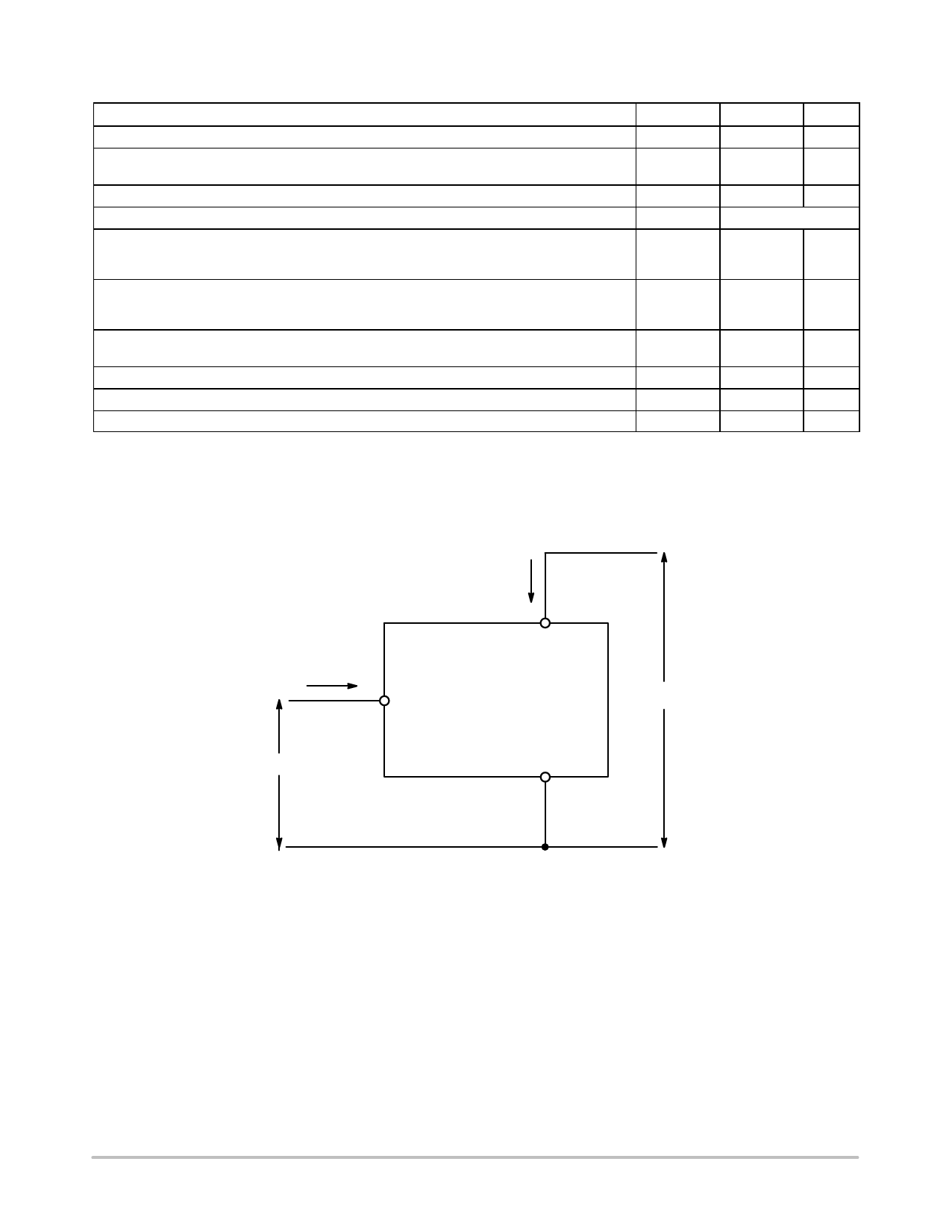
+
ID
IG
+
VGS
GATE
DRAIN
SOURCE
VDS
−
−
Figure 1. Voltage and Current Convention
http://onsemi.com
2
Share Link: 