SA572D データシートの表示(PDF) - Philips Electronics
部品番号
コンポーネント説明
メーカー
SA572D Datasheet PDF : 8 Pages
| |||
Philips Semiconductors RF Communications Products
Programmable analog compandor
Product specification
NE/SA572
VREF
+
A2
–
R2
VIN
V+
IR
+
VIN *
VREF
R2
Q5
D7
Q6
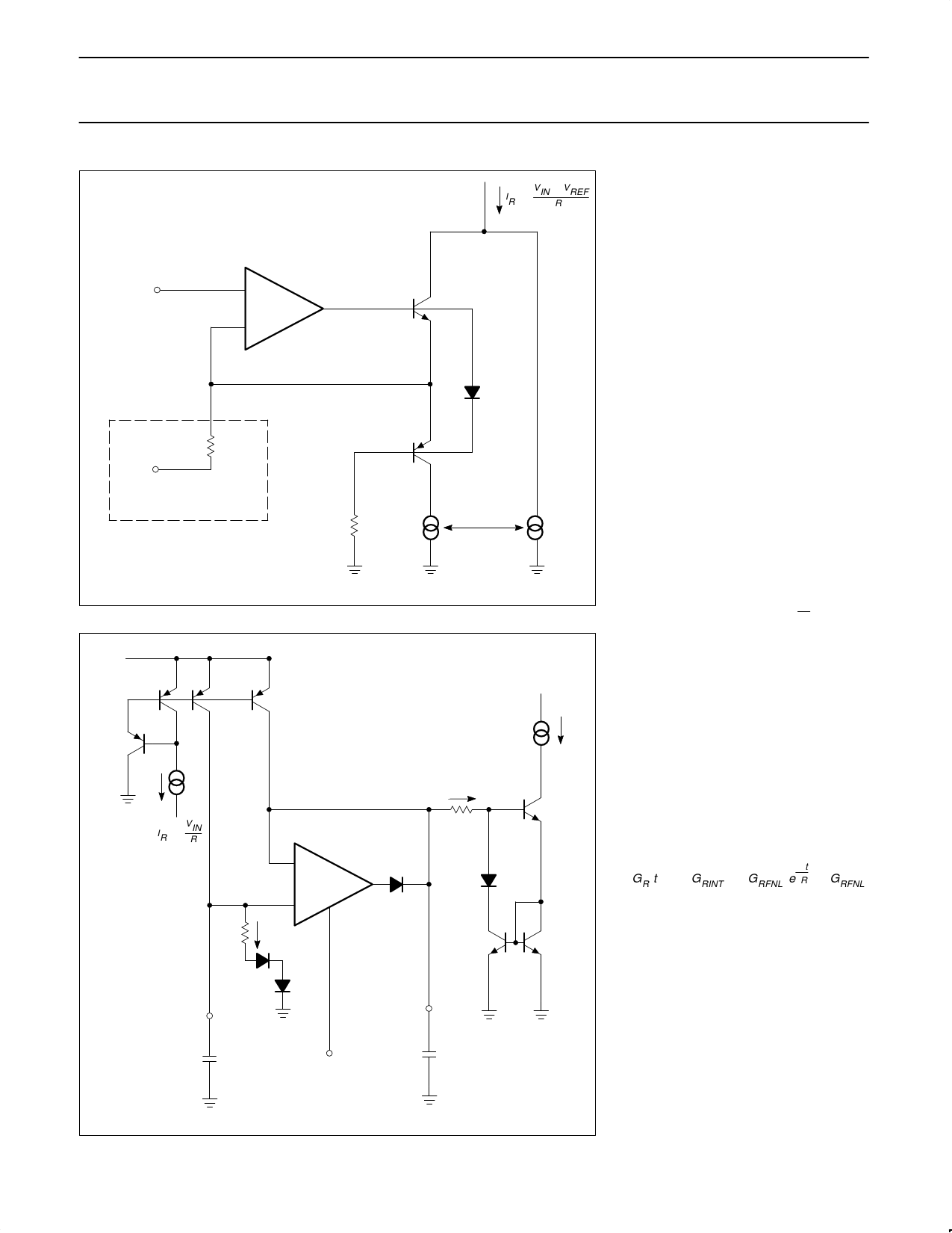
Figure 2. Simplified Rectifier Schematic
Q8 Q9
V+
Q10
Q17
IR
+
VIN
R
10k
–
A3
+
IR1
D11
D12
IQ = 2IR2
IR2
X2
Q16
10k
D15
D13
Q14
X2
Q18
CR
CA
TRACKING
TRIM
Figure 3. Buffer Amplifier Schematic
Buffer Amplifier
In audio systems, it is desirable to have fast
attack time and slow recovery time for a tone
burst input. The fast attack time reduces
transient channel overload but also causes
low-frequency ripple distortion. The
low-frequency ripple distortion can be
improved with the slow recovery time. If
different attack times are implemented in
corresponding frequency spectrums in a split
band audio system, high quality performance
can be achieved. The buffer amplifier is
designed to make this feature available with
minimum external components. Referring to
Figure 3, the rectifier output current is
mirrored into the input and output of the
unipolar buffer amplifier A3 through Q8, Q9
and Q10. Diodes D11 and D12 improve
tracking accuracy and provide
common-mode bias for A3. For a
positive-going input signal, the buffer
amplifier acts like a voltage-follower.
Therefore, the output impedance of A3 makes
the contribution of capacitor CR to attack time
insignificant. Neglecting diode impedance,
the gain Ga(t) for ∆G can be expressed as
follows:
*t
Ga(t) + (GaINT * GaFNL e t A ) GaFNL
GaINT=Initial Gain
GaFNL=Final Gain
τA=RA • CA=10k • CA
where τA is the attack time constant and RA
is a 10k internal resistor. Diode D15 opens
the feedback loop of A3 for a negative-going
signal if the value of capacitor CR is larger
than capacitor CA. The recovery time
depends only on CR • RR. If the diode
impedance is assumed negligible, the
dynamic gain GR (t) for ∆G is expressed as
follows.
*t
GR(t) + (GRINT * GRFNL et R ) GRFNL
GR(t)=(GR INT–GR FNL) e +GR FNL
τR=RR • CR=10k • CR
where τR is the recovery time constant and
RR is a 10k internal resistor. The gain control
current is mirrored to the gain cell through
Q14. The low level gain errors due to input
bias current of A2 and A3 can be trimmed
through the tracking trim pin into A3 with a
current source of ±3µA.
Basic Expandor
Figure 4 shows an application of the circuit as
a simple expandor. The gain expression of
the system is given by
October 7, 1987
6
Share Link: 