NJG1106KB2 データシートの表示(PDF) - Japan Radio Corporation
部品番号
コンポーネント説明
メーカー
NJG1106KB2 Datasheet PDF : 11 Pages
| |||
NJG1106KB2
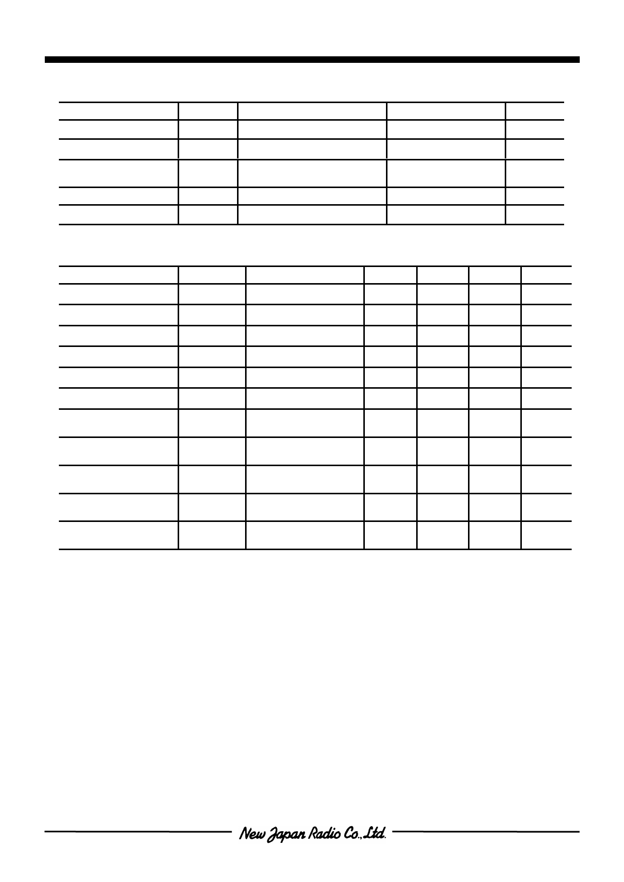
nABSOLUTE MAXIMUM RATINGS
PARAMETER
Drain Voltage
Input Power
Power Dissipation
Operating Temp.
Storage Temp.
SYMBOL
CONDITIONS
VDD
Pin
VDD=2.7V
PD
Tj=125°C, mount on PCB
FR4 20X20X0.2mm
Topr
Tstg
(Ta=+25°C, Zs=Zl=50Ω)
RATINGS
UNITS
6.0
V
+15
dBm
450
mW
-40 ~ +85
°C
-55 ~ +125
°C
nELECTRICAL CHARACTERISTICS
PARAMETER
SYMBOL
(VDD=2.7V, f=820MHz, Ta=+25°C, Zs=Zl=50Ω)
CONDITIONS
MIN
TYP
MAX UNITS
Operating frequency
freq
800
820
1000 MHz
Drain voltage
Operating current
Small signal gain
VDD
IDD
Gain
RF OFF
2.5
2.7
5.5
V
-
2.5
3.4
mA
15.0
17.0
19.0
dB
Gain flatness
Noise figure
Pout at 1dB gain
compression point
Input 3rd order
Intercept point
Output 3rd order
Intercept point
RF Input port
VSWR
RF Output port
VSWR
Gflat
f=810~885MHz
NF
-
0.5
1.0
-
1.3
1.5
P-1dB
VDD=2.7V, f=820MHz -4.0
0.0
-
IIP3 f=820.0+820.1MHz
-8.0
-4.0
-
OIP3 f=820.0+820.1MHz +9.0 +13.0
-
VSWRi VDD=2.7V, f=820MHz
-
VSWRo VDD=2.7V, f=820MHz
-
1.5
2.0
1.5
2.0
dB
dB
dBm
dBm
dBm
-2-
Share Link: 