TC429 データシートの表示(PDF) - TelCom Semiconductor Inc => Microchip
部品番号
コンポーネント説明
メーカー
TC429 Datasheet PDF : 7 Pages
| |||
6A SINGLE HIGH-SPEED,
CMOS POWER MOSFET DRIVER
1
TC429
Three components make up total package power dissi-
pation:
(1) Capacitive load dissipation (PC)
(2) Quiescent power (PQ)
(3) Transition power (PT)
The capacitive load-caused dissipation is a direct func-
tion of frequency, capacitive load, and supply voltage. The
package power dissipation is:
PC = f C VS2,
where: f = Switching frequency
C = Capacitive load
VS = Supply voltage.
Quiescent power dissipation depends on input signal
duty cycle. A logic low input results in a low-power dissipa-
tion mode with only 0.5 mA total current drain. Logic high
signals raise the current to 5 mA maximum. The quiescent
power dissipation is:
PQ = VS (D (IH) + (1–D) IL),
where: IH = Quiescent current with input high (5 mA max)
IL = Quiescent current with input low (0.5 mA max)
D = Duty cycle.
Transition power dissipation arises because the output
stage N- and P-channel MOS transistors are ON simulta-
neously for a very short period when the output changes.
The transition package power dissipation is approximately:
PT = f VS (3.3 x 10⁻⁹ A · Sec).
An example shows the relative magnitude for each item.
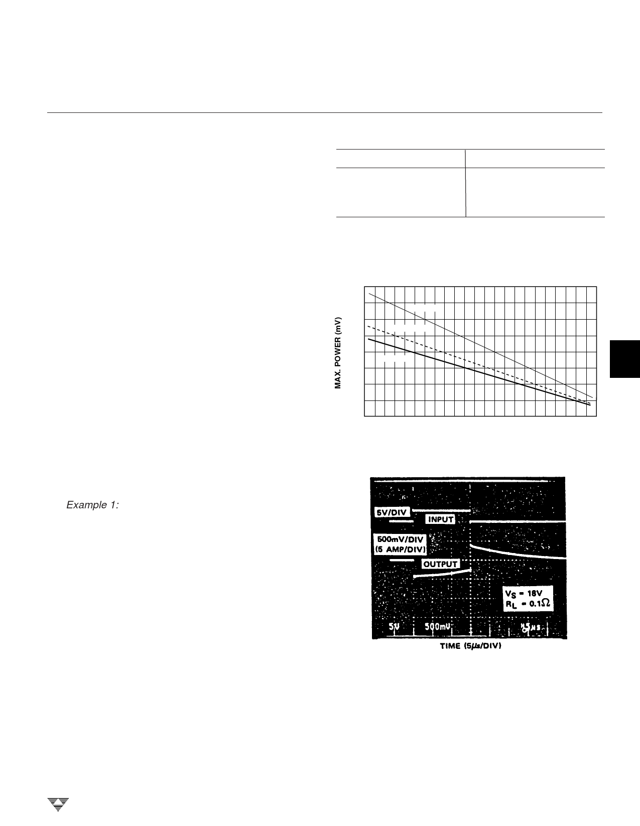
Example 1:
C = 2500 pF
VS = 15V
D = 50%
f = 200 kHz
PD = Package power dissipation = PC + PT + PQ
= 113 mW + 10 mW + 41 mW
= 164 mW.
Maximum operating temperature = TJ – θJA (PD)
= 125°C,
where: TJ = Maximum allowable junction temperature
(+150°C)
θJA = Junction-to-ambient thermal resistance
(150°C/W, CerDIP).
NOTE: Ambient operating temperature should not exceed +85°C for
IJA devices or +125°C for MJA devices.
TELCOM SEMICONDUCTOR, INC.
Table 1. Maximum Operating Frequencies
VS
fMax
18V
500 kHz
15V
700 kHz
10V
1.3 MHz
5V
>2 MHz
CONDITIONS: 1. CerDIP Package (θJA = 150°C/W)
2. TA = +25°C
3. CL = 2500 pF
Thermal Derating Curves
1600
1400
1200
1000
8 Pin DIP
8 Pin CerDIP
800
8 Pin SOIC
600
400
200
0
0 10 20 30 40 50 60 70 80 90 100 110 120
AMBIENT TEMPERATURE (°C)
2
3
4
Peak Output Current Capability
5
6
POWER-ON OSCILLATION
7
It is extremely important that all MOSFET DRIVER
applications be evaluated for the possibility of having
HIGH-POWER OSCILLATIONS occurring during the
POWER-ON cycle.
POWER-ON OSCILLATIONS are due to trace size and
layout as well as component placement. A ‘quick fix’ for most
8 applications which exhibit POWER-ON OSCILLATION prob-
lems is to place approximately 10 kΩ in series with the input
of the MOSFET driver.
4-179
Share Link: 