NJM3517E2 データシートの表示(PDF) - Japan Radio Corporation
部品番号
コンポーネント説明
メーカー
NJM3517E2 Datasheet PDF : 12 Pages
| |||
NJM3517
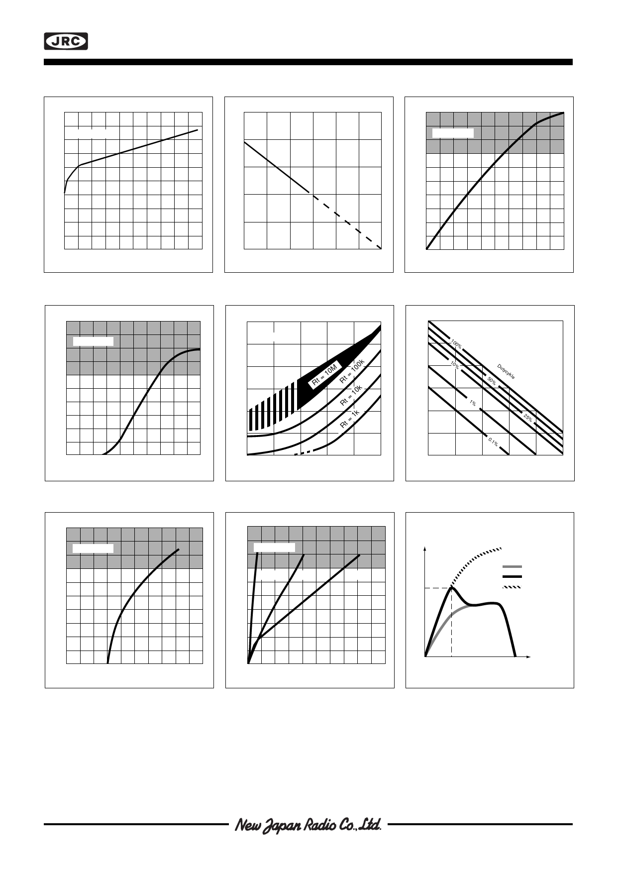
s TYPICAL CHARACTERISTICS
VLCE sat [V]
2.5
2.0 TA= +25° C
Allowable power dissipation [W]
2.5
2.0
Output Current [A]
0.5
TA= +25° C
0.4
1.5
1.5
0.3
1.0
1.0
0.2
0,5
0,5
0.1
0
0
0.1
0.2
0.3
0.4
0.5
IL [A]
Figure 17. Typical second output
saturation voltage vs. output current
Output Current [mA]
10
TA= +25° C
8
6
4
2
0
0
0.2
0.4
0.6
0.8 1.0
Output Voltage [V]
Figure 20. Typical IØ vs. VØCE Sat. “Zero
output” saturation
Output Current [A]
0.5
TA= +25° C
0.4
(IL= 0)
0.3
0.2
0
0
50
100
150
Ambient temrature [°C]
0
0
0.2
0.4
0.6
0.8 1.0
Output Voltage [V]
Figure 18. Power dissipation vs. Ambient Figure 19. Typical phase output satura-
temrature.
tion voltage vs. output current
Output Pulse Width [s]
1
TA= +25° C
10 -1
10 -2
10 -3
Rt = 10M
Rt = 100k
Rt = 10k
10 -4
Rt = 1k
10 -5
10 -6
0.01
0.1
1
10
100
Ct Capacitance [nF]
1000
Figure 21. Typical t vs. C /R . Output
On
TT
pulse width vs. capacitance/resistance
Output Current [A]
-0.5
TA= +25° C
-0.4
(Ip = 0)
10%
-0.3
50%
100%
-0.2
Output Pulse Width [s]
1
10 -1
100%
TA= +25° C
10 -2
10 -3
10 -4
10%
50% Dutycykle
1%
25%
10 -5
0.1%
10 -6
0.001 0.01
0.1
1
10 100
fs Step frequency [kHz]
Figure 22.Typical ton vs. fs/dc. Output
pulse width vs.step frequency/duty
Motor Current [mA]
350
Normal
Bilevel
Bilevel without
time limit
0.1
-0.1
0
0
0.2
0.4
0.6
0.8 1.0
Power Dissipation [W]
0
0
0.2
0.4
0.6
0.8 1.0
Power Dissipation [W]
Figure 23. Typical PDP vs. IP. Power
dissipation without second-level supply
Figure 24. Typical PDL vs. IL. Power
dissipation in the bilevel pulse when
(includes 2 active outputs = FULL STEP) raising to the IL value. One active output
tON
Time
Figure 25 . Motor Current IP
Share Link: 