NJU7333 データシートの表示(PDF) - Japan Radio Corporation
部品番号
コンポーネント説明
メーカー
NJU7333 Datasheet PDF : 6 Pages
| |||
NJU7333
Preliminary
Given that the bias current is set to be 5mA by HW101A datasheet, R1 and R2 can be determined as follows:
R1+ R2 + Rin
=
VDD
Ihbias
=
5
5 ×10−3
= 1kΩ
R1 = R2 = 300Ω
The output voltage of hall elements is influenced by the bias current and magnetic flux density of hall elements.
The optimum input voltage of NJU7333 is 100mVp-p and higher. With such input voltage, the highest efficiency can
be obtained.
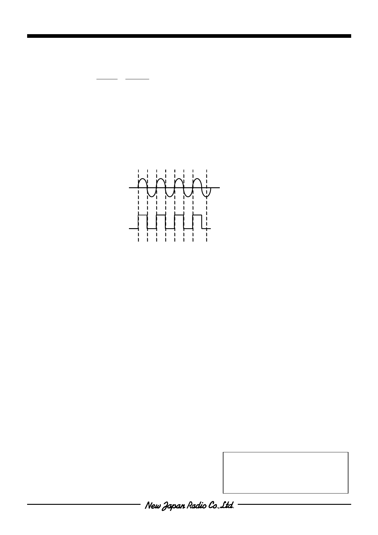
4. Design of FG output resistsnce (R3)
FG Out(FG:Pin2) is a open drain output and R3 is a pull up register. A typical value of R3 is 10kΩ. The timing chart
of FG Out is as follows.
Hall input
IN+
FG Terminal voltage
-6-
The specifications on this data book are only given for
information, without any guarantee as regards either mistakes or
omissions. The application circuit in this data book are described
only to show representative usages of the product and not
intended for the guarantee or permission of any right including
the industrial rights.
Share Link: 