SPT7862 データシートの表示(PDF) - Signal Processing Technologies
部品番号
コンポーネント説明
メーカー
SPT7862 Datasheet PDF : 10 Pages
| |||
• Since only 16 comparators are used, a huge power sav-
ings is realized.
• The auto-zero operation is done using a closed loop sys-
tem that uses multiple samples of the comparator’s
response to a reference zero.
• The auto-calibrate operation, which calibrates the gain
of the MSB reference and the LSB reference, is also
done with a closed loop system. Multiple samples of
the gain error are integrated to produce a calibration volt-
age for each SAR ADC section.
• Capacitive displacement currents, which can induce sam-
pling error, are minimized since only one comparator
samples the input during a clock cycle.
• The total input capacitance is very low, since sections of
the converter which are not sampling the signal are iso-
lated from the input by transmission gates.
VOLTAGE REFERENCE
The SPT7862 requires the use of a single external voltage
reference for driving the high side of each reference ladder.
Each ladder is totally independent and may operate at dif-
ferent voltage levels. The high side of the reference ladder
must operate within a range of 3 V to 5 V. The lower side of
each ladder is typically tied to AGND (0.0 V), but can be run
up to 2.0 V with a second reference. The analog input volt-
age range will track the total voltage difference measured
between the ladder sense lines, VRHS and VRLS.
Force and sense taps are provided to ensure accurate and
stable setting of the upper and lower ladder sense line volt-
ages across part-to-part and temperature variations. By
using the configuration shown in figure 3, offset and gain
errors of less than ±2 LSB can be obtained.
In cases in which wider variations in offset and gain can be
tolerated, the external reference can be tied directly to VRHF
and AGND can be tied directly to VRLF as shown in figure 4.
Decouple force and sense lines to AGND with a .01 µF ca-
pacitor (chip cap preferred) to minimize high-frequency
noise injection. If this simplified configuration is used, the
following considerations should be taken into account:
The reference ladder circuit shown in figure 4 is a simplified
representation of the actual reference ladder with force and
sense taps shown. Due to the actual internal structure of the
ladder, the voltage drop from VRHF to VRHS is not equivalent
to the voltage drop from VRLF to VRLS.
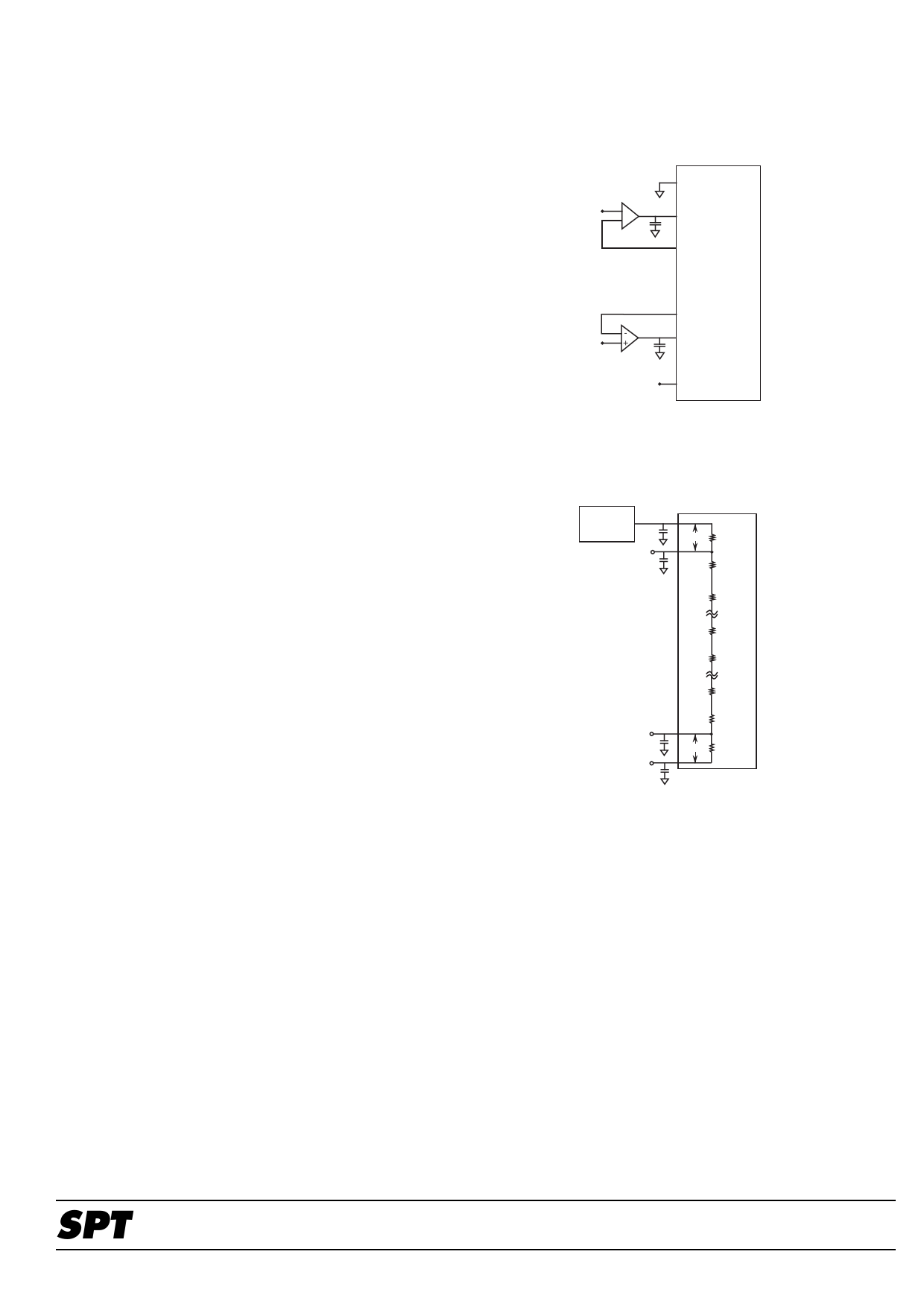
Figure 3 – Ladder Force/Sense Circuit for Each ADC
1 AGND
+
-
2 VRHF
3 VRHS
4 N/C
5 VRLS
-
+
6 VRLF
7 VIN
All capacitors are 0.01 µF
Figure 4 – Simplified Reference Ladder Drive Circuit
Without Force/Sense Circuit
+4.0 V
External
Reference
VRHS
(+3.91 V)
90 mV R/2
R
R
VRLS
(0.075 V)
VRLF (AGND)
0.0 V
R
R
R
R
75 mV R/2
R=30 Ω (typ)
All capacitors are 0.01 µF
Typically, the top side voltage drop for VRHF to VRHS will
equal:
VRHF – VRHS = 2.25 % of (VRHF – VRLF) (typical),
and the bottom side voltage drop for VRLS to VRLF will equal:
VRLS – VRLF = 1.9 % of (VRHF – VRLF) (typical).
Figure 4 shows an example of expected voltage drops for a
specific case. VREF of 4.0 V is applied to VRHF and VRLF is
tied to AGND. A 90 mV drop is seen at VRHS (= 3.91 V) and
a 75 mV increase is seen at VRLS (= 0.075 V).
SPT
7
SPT7862
2/23/00
Share Link: 