NM25C040 データシートの表示(PDF) - Fairchild Semiconductor
部品番号
コンポーネント説明
メーカー
NM25C040
Fairchild Semiconductor

NM25C040 Datasheet PDF : 10 Pages
| |||
Functional Description
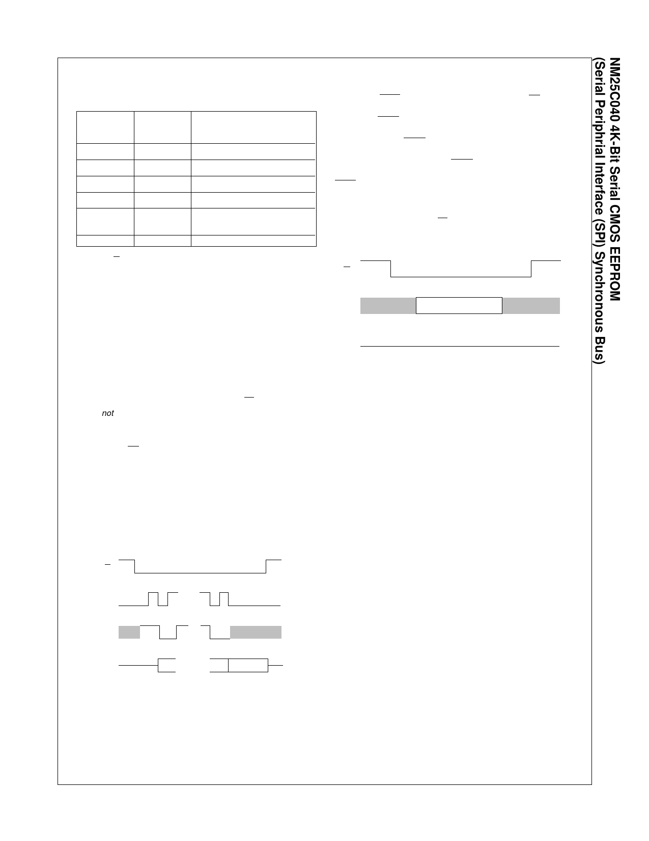
TABLE 1. Instruction Set
Instruction Instruction
Name Opcode
Operation
WREN
00000110 Set Write Enable Latch
WRDI
00000100 Reset Write Enable Latch
RDSR
00000101 Read Status Register
WRSR
00000001 Write Status Register
READ
0000A011
Read Data from Memory
Array
WRITE
0000A010 Write Data to Memory Array
Note: As the NM25C040 requires 9 address bits (4,096 ÷ 8 = 512 bytes = 29), the
9th bit (for R/W instructions) is inputted in the Instruction Set Byte in bit I3. This
convention only applies to 4K SPI protocol.
MASTER: The device that generates the serial clock is desig-
nated as the master. The NM25C040 can never function as a
master.
SLAVE: The NM25C040 always operates as a slave as the serial
clock pin is always an input.
TRANSMITTER/RECEIVER: The NM25C040 has separate pins
for data transmission (SO) and reception (SI).
HOLD: The HOLD pin is used in conjunction with the CS to select
the device. Once the device is selected and a serial sequence is
underway, HOLD may be forced low to suspend further serial
communication with the device without resetting the serial se-
quence. Note that HOLD must be brought low while the SCK pin
is low. The device must remain selected during this sequence. To
resume serial communication HOLD is brought high while the
SCK pin is low. The SO pin is at a high impedance state during
HOLD.
INVALID OP-CODE: After an invalid code is received, no data is
shifted into the NM25C040, and the SO data output pin remains
high impedance until a new CS falling edge reinitializes the serial
communication. See Figure 5.
FIGURE 5. Invalid Op-Code
CS
SI
INVALID CODE
SO
DS012401-7
MSB: The Most Significant Bit is the first bit transmitted and
received.
CHIP SELECT: The chip is selected when pin CS is low. When the
chip is not selected, data will not be accepted from pin SI, and the
output pin SO is in high impedance.
SERIAL OP-CODE: The first byte transmitted after the chip is
selected with CS going low contains the op-code that defines the
operation to be performed.
PROTOCOL: When connected to the SPI port of a 68HC11
microcontroller, the NM25C040 accepts a clock phase of 0 and a
clock polarity of 0. The SPI protocol for this device defines the byte
transmitted on the SI and SO data lines for proper chip operation.
See Figure 4.
FIGURE 4. SPI Protocol
CS
SCK
…
SI
Bit 7 Bit 6 … Bit 0
SO
Bit 7 … Bit 1 Bit 0
DS012401-5
Data is clocked in on the positive SCK edge and out on the
negative SCK edge.
NM25C040 Rev. D.1
6
www.fairchildsemi.com
Share Link: