NM25C040 データシートの表示(PDF) - Fairchild Semiconductor
部品番号
コンポーネント説明
メーカー
NM25C040
Fairchild Semiconductor

NM25C040 Datasheet PDF : 10 Pages
| |||
Functional Description (Continued)
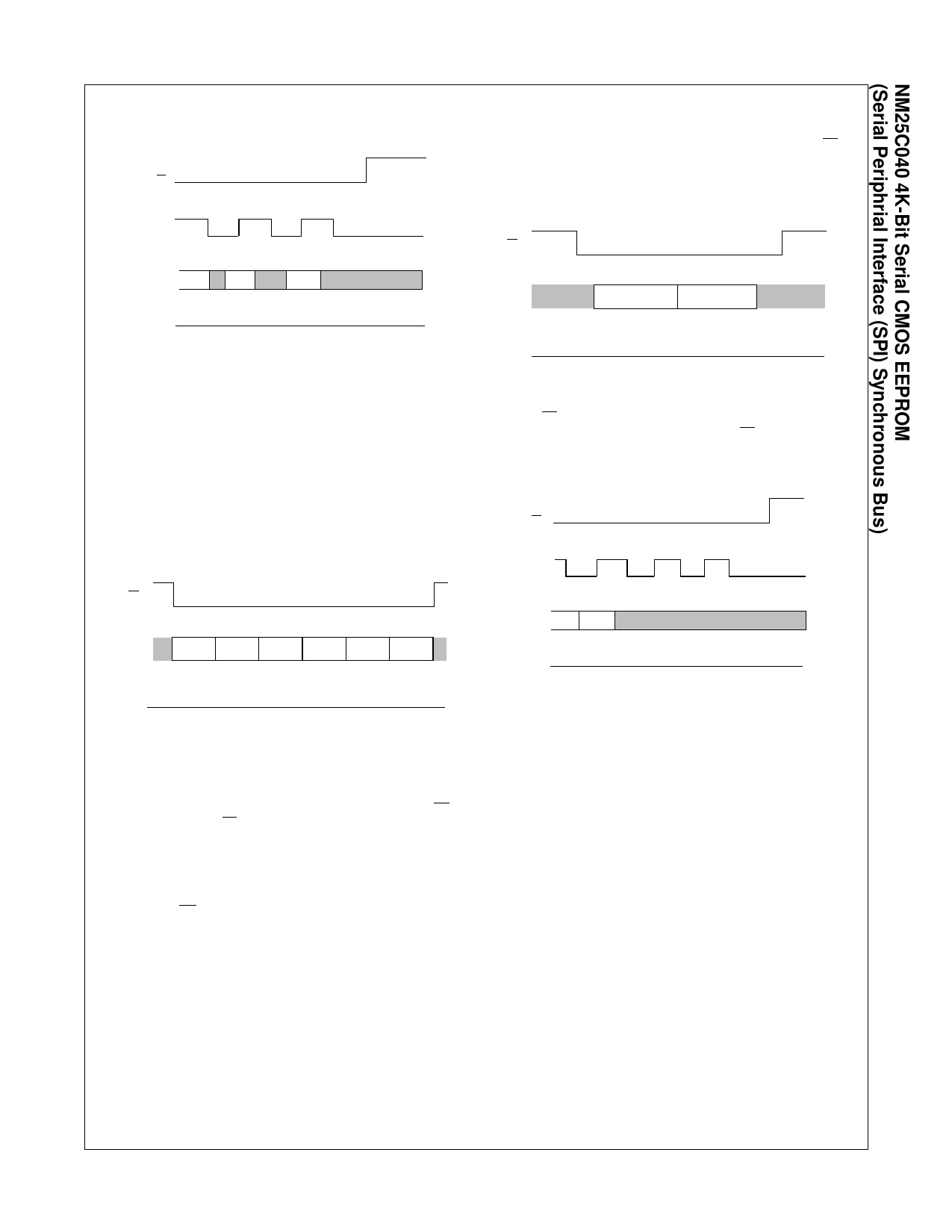
FIGURE 10. Write Sequence
The WRSR command requires the following sequence. The CS
line is pulled low to select the device and then the WRSR op-code
CS
is transmitted on the SI line followed by the data to be pro-
grammed. See Figure 12.
FIGURE 12. Write Status Register
SCK
CS
SI D2
D1
D0
SI
SO
DS012401-12
The READY/BUSY status of the device can be determined by
SO
WRSR
SR Data
Op-Code xxxxBP1BP0xx
DS012401-14
executing a READ STATUS REGISTER (RDSR) instruction. Bit 0
= 1 indicates that the WRITE cycle is still in progress and Bit 0 = Note that the first four bits are don’t care bits followed by BP1 and
0 indicates that the WRITE cycle has ended. During the WRITE BP0 then two additional don’t care bits. Programming will start
programming cycle (Bit 0 = 1) only the READ STATUS REGIS- after the CS pin is forced back to a high level. As in the WRITE
TER instruction is enabled.
instruction the LOW to HIGH transition of the CS pin must occur
during the SCK low time immediately after clocking in the last don’t
The NM25C040 is capable of a 4 byte PAGE WRITE operation. care bit. See Figure 13.
After receipt of each byte of data the two low order address bits are
internally incremented by one. The seven high order bits of the
FIGURE 13. Start WRSR Condition
address will remain constant. If the master should transmit more
than 4 bytes of data, the address counter will “roll over,” and the
CS
previously loaded data will be reloaded. See Figure 11.
FIGURE 11. 4 Byte Page Write
CS
Write
Byte
Data
Data
Data
Data
SI
Op-Code Addr (n) (n)
(n + 1) (n + 2) (n + 3)
SO
SCK
SI
BP0
SO
DS012401-15
The READY/BUSY status of the device can be determined by
executing a READ STATUS REGISTER (RDSR) instruction. Bit 0
DS012401-13 = 1 indicates that the WRSR cycle is still in progress and Bit 0 =
0 indicates that the WRSR cycle has ended.
At the completion of a WRITE cycle the device is automatically
returned to the write disable state.
At the completion of a WRITE cycle the device is automatically
returned to the write disable state.
If the device is not WRITE enabled, the device will ignore the
WRITE instruction and return to the standby state when CS is
forced high. A new CS falling edge is required to re-initialize the
serial communication.
WRITE STATUS REGISTER (WRSR): The WRITE STATUS
REGISTER (WRSR) instruction is used to program the non-
volatile status register Bits 2 and 3 (BP0 and BP1). The WRITE
PROTECT (WP) pin must be held high and two separate instruc-
tions must be executed. The chip must first be write enabled via
the WRITE ENABLE instruction and then a WRSR instruction
must be executed.
NM25C040 Rev. D.1
8
www.fairchildsemi.com
Share Link: