NM27C64 データシートの表示(PDF) - Fairchild Semiconductor
部品番号
コンポーネント説明
メーカー
NM27C64 Datasheet PDF : 10 Pages
| |||
Functional Description
DEVICE OPERATION
The six modes of operation of the NMC27C64 are listed in Table
1. It should be noted that all inputs for the six modes are at TTL
levels. The power supplies required are VCC and VPP. The VPP
power supply must be at 12.75V during the three programming
modes, and must be at 5V in the other three modes. The VCC
power supply must be at 6V during the three programming modes,
and at 5V in the other three modes.
Read Mode
The NMC27C64 has two control functions, both of which must be
logically active in order to obtain data at the outputs. Chip Enable
(CE) is the power control and should be used for device selection.
Output Enable (OE) is the output control and should be used to
gate data to the output pins, independent of device selection. The
programming pin (PGM) should be at VIH except during program-
ming. Assuming that addresses are stable, address access time
(tACC) is equal to the delay from CE to output (tCE). Data is available
at the outputs tOE after the falling edge of OE , assuming that CE
has been low and addresses have been stable for at least tACC –
tOE.
The sense amps are clocked for fast access time. VCC should
therefore be maintained at operating voltage during read and
verify. If VCC temporarily drops below the spec. voltage (but not to
ground) an address transition must be performed after the drop to
insure proper output data.
Standby Mode
The NMC27C64 has a standby mode which reduces the active
power dissipation by 99%, from 55 mW to 0.55 mW. The
NMC27C64 is placed in the standby mode by applying a CMOS
high signal to the CE input. When in standby mode, the outputs are
in a high impedance state, independent of the OE input.
Output OR-Tying
Because NMC27C64s are usually used in larger memory arrays,
Fairchild has provided a 2-line control function that accommo-
dates this use of multiple memory connections. The 2-line control
function allows for:
1. the lowest possible memory power dissipation, and
2. complete assurance that output bus contention will not
occur.
To most efficiently use these two control lines, it is recomended
that CE (pin 20) be decoded and used as the primary device
selecting function, while OE (pin 22) be made a common connec-
tion to all devices in the array and connected to the READ line from
the system control bus. This assures that all deselected memory
devices are in their low power standby modes and that the output
pins are active only when data is desired from a particular memory
device.
Programming
CAUTION: Exceeding 14V on pin 1 (VPP) will damage the
NMC27C64.
Initially, all bits of the NMC27C64 are in the “1” state. Data is
introduced by selectively programming “0s” into the desired bit
locations. Although only “0s” will be programmed, both “1s” and
“0s” can be presented in the data word. A “0” cannot be changed
to a “1” once the bit has been programmed.
The NMC27C64 is in the programming mode when the VPP power
supply is at 12.75V and OE is at VIH. It is required that at least a
0.1 F capacitor be placed across VPP, VCC to ground to suppress
spurious voltage transients which may damage the device. The
data to be programmed is applied 8 bits in parallel to the data
output pins. The levels required for the address and data inputs
are TTL.
For programming, CE should be kept TTL low at all times while VPP
is kept at 12.75V.
When the address and data are stable, an active low, TTL program
pulse is applied to the PGM input. A program pulse must be
applied at each address location to be programmed. The
NMC27C64 is programmed with the Fast Programming Algorithm
shown in Figure 1. Each address is programmed with a series of
100 s pulses until it verfies good, up to a maximum of 25 pulses.
Most memory cells will program with a single 100 s pulse. The
NMC27C64 must not be programmed with a DC signal applied to
the PGM input.
Programming multiple NMC27C64s in parallel with the same data
can be easily accomplished due to the simplicity of the program-
ming requirements. Like inputs of the paralleled NMC27C64s may
be connected together when they are programmed with the same
data. A low level TTL pulse applied to the PGM input programs the
paralleled NMC27C64s. If an application requires erasing and
reprogramming, the NMC27C64Q UV erasable PROM in a win-
dowed package should be used.
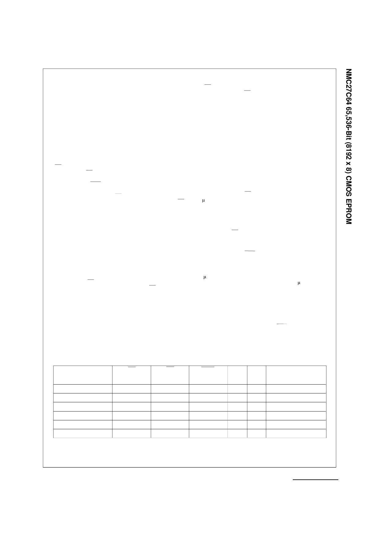
Mode
Pins
Read
Standby
Output Disable
Program
Program Verify
Program Inhibit
CE
(20)
VIL
VIH
Don’t Care
VIL
VIL
VIH
TABLE 1. Mode Selection
OE
(22)
VIL
Don’t Care
VIH
VIH
VIL
Don’t Care
PGM
(27)
VIH
Don’t Care
VIH
VIH
Don’t Care
VPP
(1)
5V
5V
5V
13V
13V
13V
VCC
(28)
5V
5V
5V
6V
6V
6V
Outputs
(11–13, 15–19)
DOUT
Hi-Z
Hi-Z
DIN
DOUT
Hi-Z
NMC27C64 Rev. C
8
www.fairchildsemi.com
Share Link: 