NM93C56EN データシートの表示(PDF) - Fairchild Semiconductor
部品番号
コンポーネント説明
メーカー
NM93C56EN
Fairchild Semiconductor

NM93C56EN Datasheet PDF : 16 Pages
| |||
Pin Description
Chip Select (CS)
This is an active high input pin to NM93CS56 EEPROM (the device)
and is generated by a master that is controlling the device. A high
level on this pin selects the device and a low level deselects the
device. All serial communications with the device is enabled only
when this pin is held high. However this pin cannot be permanently
tied high, as a rising edge on this signal is required to reset the
internal state-machine to accept a new cycle and a falling edge to
initiate an internal programming after a write cycle. All activity on the
SK, DI and DO pins are ignored while CS is held low.
Serial Clock (SK)
This is an input pin to the device and is generated by the master that
is controlling the device. This is a clock signal that synchronizes the
communication between a master and the device. All input informa-
tion (DI) to the device is latched on the rising edge of this clock input,
while output data (DO) from the device is driven from the rising edge
of this clock input. This pin is gated by CS signal.
Serial Input (DI)
This is an input pin to the device and is generated by the master
that is controlling the device. The master transfers Input informa-
tion (Start bit, Opcode bits, Array addresses and Data) serially via
this pin into the device. This Input information is latched on the
rising edge of the SCK. This pin is gated by CS signal.
Serial Output (DO)
This is an output pin from the device and is used to transfer Output
data via this pin to the controlling master. Output data is serially
shifted out on this pin from the rising edge of the SCK. This pin is
active only when the device is selected.
Protect Register Enable (PRE)
This is an active high input pin to the device and is used to
distinguish operations to memory array and operations to Protect
Register. When this pin is held low, operations to the memory
array are enabled. When this pin is held high, operations to the
Protect Register are enabled. This pin operates in conjunction
with PE pin. Refer Table1 for functional matrix of this pin for
various operations.
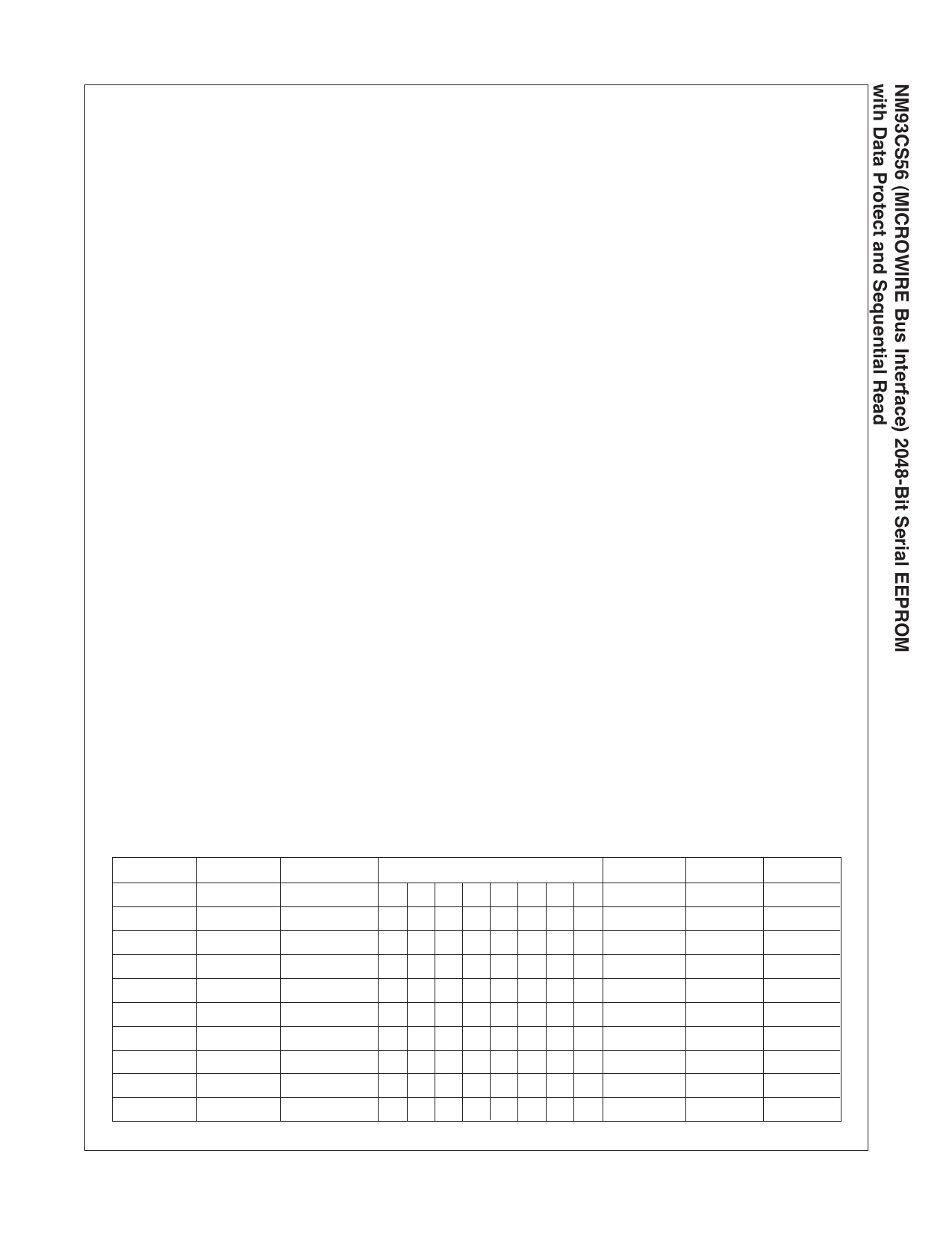
TABLE 1. Instruction set
Program Enable (PE)
This is an active high input pin to the device and is used to enable
operations, that are write in nature, to the memory array and to the
Protect register. When this pin is held high, operations that are
“write” in nature are enabled. When this pin is held low, operations
that are “write” in nature are disabled. This pin operates in
conjunction with PRE pin. Refer Table1 for functional matrix of this
pin for various operations.
Microwire Interface
A typical communication on the Microwire bus is made through the
CS, SK, DI and DO signals. To facilitate various operations on the
Memory array and on the Protect Register, a set of 10 instructions
are implemented on NM93CS56. The format of each instruction is
listed in Table 1.
Instruction
Each of the above 10 instructions is explained under individual
instruction descriptions.
Start Bit
This is a 1-bit field and is the first bit that is clocked into the device
when a Microwire cycle starts. This bit has to be “1” for a valid cycle
to begin. Any number of preceding “0” can be clocked into the
device before clocking a “1”.
Opcode
This is a 2-bit field and should immediately follow the start bit.
These two bits (along with PRE, PE signals and 2 MSB of address
field) select a particular instruction to be executed.
Address Field
This is a 8-bit field and should immediately follow the Opcode bits.
In NM93CS56, only the LSB 7 bits are used for address decoding
during READ, WRITE and PRWRITE instructions. During these
three instructions (READ, WRITE and PRWRITE), the MSB is
“don’t care” (can be 0 or 1). During all other instructions (with the
exception of PRREAD), the MSB 2 bits are used to decode
instruction (along with Opcode bits, PRE and PE signals).
Data Field
This is a 16-bit field and should immediately follow the Address
bits. Only the WRITE and WRALL instructions require this field.
D15 (MSB) is clocked first and D0 (LSB) is clocked last (both
during writes as well as reads).
Instruction
READ
WEN
WRITE
WRALL
WDS
PRREAD
PREN
PRCLEAR
PRWRITE
PRDS
Start Bit Opcode Field
Address Field
Data Field PRE Pin
1
10
X A6 A5 A4 A3 A2 A1 A0
0
1
00
1 1XXXXXX
0
1
01
X A6 A5 A4 A3 A2 A1 A0 D15-D0
0
1
00
0 1 X X X X X X D15-D0
0
1
00
0 0XXXXXX
0
1
10
XXXXXXXX
1
1
00
1 1XXXXXX
1
1
11
11111111
1
1
01
X A6 A5 A4 A3 A2 A1 A0
1
1
00
00000000
1
PE Pin
X
1
1
1
X
X
1
1
1
1
NM93CS56 Rev. F.2
5
www.fairchildsemi.com
Share Link: