SSM2211P データシートの表示(PDF) - Analog Devices
部品番号
コンポーネント説明
メーカー
SSM2211P Datasheet PDF : 16 Pages
| |||
SSM2211
For an application where R1 = 10 kΩ and CC = 0.22 µF, the
midrail bypass capacitor, CB, should be at least 0.1 µF to mini-
mize start-up popping noise.
SSM2211 Amplifier Design Example
Given:
Maximum Output Power
Input Impedance
Load Impedance
Input Level
Bandwidth
1W
20 kΩ
8Ω
1 V rms
20 Hz – 20 kHz ± 0.25 dB
The configuration shown in Figure 39 will be used. The first
thing to determine is the minimum supply rail necessary to ob-
tain the specified maximum output power. From Figure 43, for
1 W of output power into an 8 Ω load, the supply voltage must
be at least 4.6 V. A supply rail of 5 V can be easily obtained
from a voltage reference. The extra supply voltage will also al-
low the SSM2211 to reproduce peaks in excess of 1 W without
clipping the signal. With VDD = 5 V and RL = 8 Ω, Equation 9
shows that the maximum power dissipation for the SSM2211 is
633 mW. From the power derating curve in Figure 28, the am-
bient temperature must be less than +85°C.
The required gain of the amplifier can be determined from
Equation 17:
AV
= PLRL
VIN , rms
= 2.8
(17)
From Equation 1,
RF =
R1
AV
2
, or
RF
= 1.4 × R1. Since the de-
sired input impedance is 20 kΩ, R1 = 20 kΩ and R2 = 28 kΩ.
The final design step is to select the input capacitor. Because add-
ing an input capacitor, CC, high pass filter, the corner frequency
needs to be far enough away for the design to meet the bandwidth
criteria. For a 1st order filter to achieve a passband response
within 0.25 dB, the corner frequency should be at least 4.14 times
away from the passband frequency. So, (4.14 ϫ fHP) < 20 Hz.
Using Equation 2, the minimum size of input capacitor can be
found:
( ) CC
>
2π
1
20
kΩ
20 Hz
4.14
(18)
So CC > 1.65 µF. Using a 2.2 µF is a practical choice for CC.
The gain-bandwidth product for each internal amplifier in the
SSM2211 is 4 MHz. Because 4 MHz is much greater than
4.14 ؋ 20 kHz, the design will meet the upper frequency band-
width criteria. The SSM2211 could also be configured for higher
differential gains without running into bandwidth limitations.
Equation 16 shows an appropriate value for CB to reduce start-
up popping noise:
( )( ) 2.2 µF 20 kΩ
CB >
25 kΩ
= 1.76 µF
(19)
Selecting CB to be 2.2 µF for a practical value of capacitor will
minimize start-up popping noise.
To summarize the final design:
VDD
R1
RF
CC
CB
Max. TA
5V
20 kΩ
28 kΩ
2.2 µF
2.2 µF
+85°C
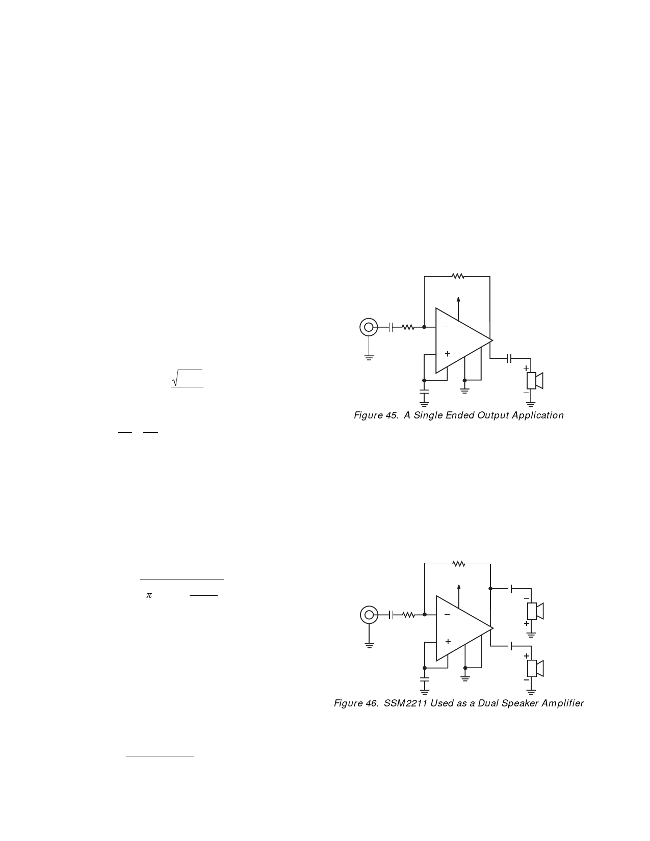
Single Ended Applications
There are applications where driving a speaker differentially is
not practical. An example would be a pair of stereo speakers
where the minus terminal of both speakers is connected to
ground. Figure 45 shows how this can be accomplished.
10k⍀
AUDIO
INPUT
+5V
10k⍀
0.47F
6
4
5
SSM2211
3
18
7
2
470F
0.1F
250mW
SPEAKER
(8⍀)
Figure 45. A Single Ended Output Application
It is not necessary to connect a dummy load to the unused output
to help stabilize the output. The 470 µF coupling capacitor cre-
ates a high pass frequency cutoff as given in Equation 4 of 42 Hz,
which is acceptable for most computer speaker applications.
The overall gain for a single ended output configuration is
AV = RF/R1, which for this example is equal to 1.
Driving Two Speakers Single Endedly
It is possible to drive two speakers single endedly with both out-
puts of the SSM2211.
20k⍀
AUDIO
INPUT
+5V
20k⍀
1F
6
4
470F
5
SSM2211
3
18
7
2
470F
0.1F
LEFT
SPEAKER
(8⍀)
RIGHT
SPEAKER
(8⍀)
Figure 46. SSM2211 Used as a Dual Speaker Amplifier
Each speaker is driven by a single ended output. The trade-off
is that only 250 mW sustained power can be put into each
speaker. Also, a coupling capacitor must be connected in series
with each of the speakers to prevent large DC currents from
flowing through the 8 Ω speakers. These coupling capacitors
–12–
REV. 0
Share Link: 