SPT7814BIJ データシートの表示(PDF) - Signal Processing Technologies
部品番号
コンポーネント説明
メーカー
SPT7814BIJ Datasheet PDF : 11 Pages
| |||
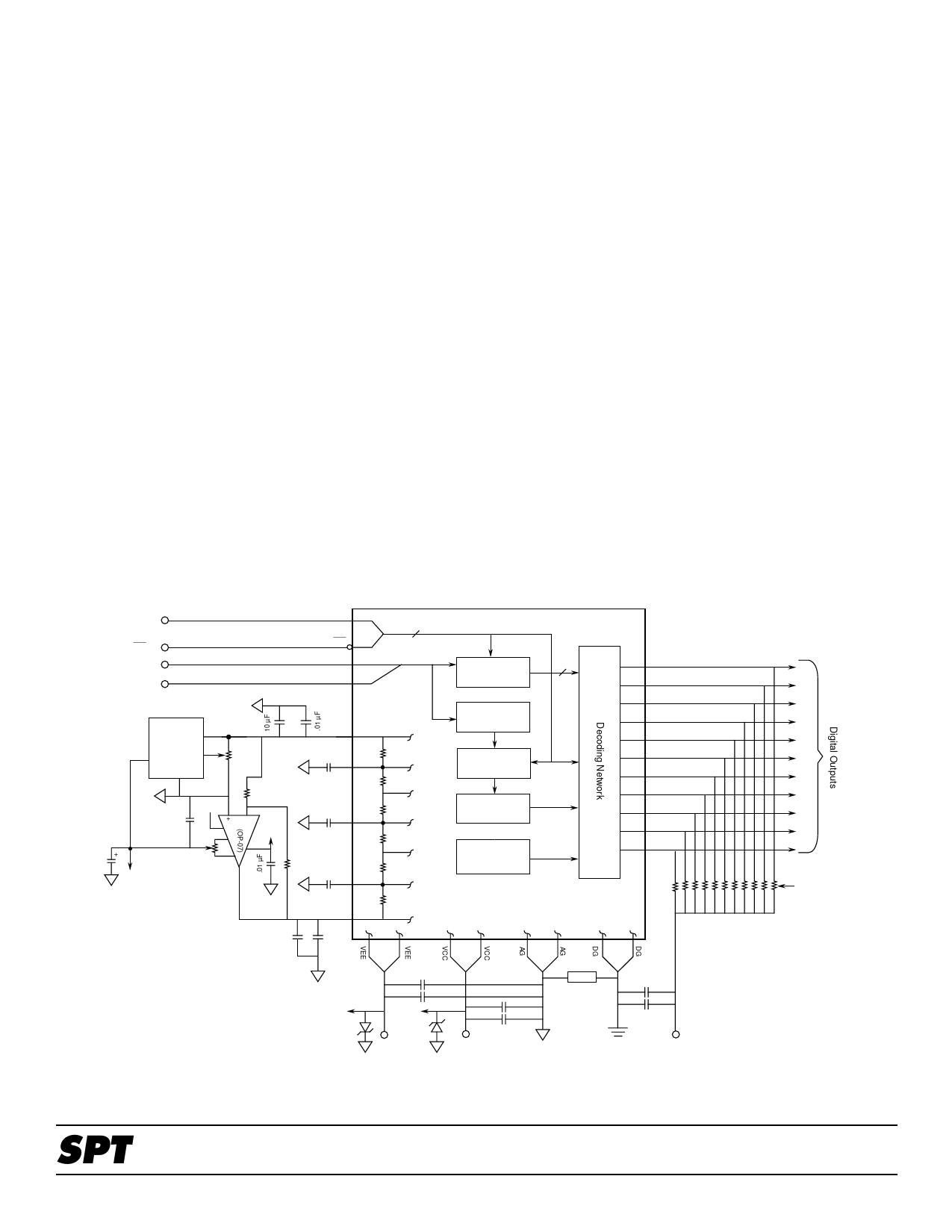
TYPICAL INTERFACE CIRCUIT
The SPT7814 requires few external components to achieve
the stated operation and performance. Figure 2 shows the
typical interface requirements when using the SPT7814 in
normal circuit operation.
The following section provides a description of the pin func-
tions and outlines critical performance criteria to consider for
achieving the optimal device performance.
POWER SUPPLIES AND GROUNDING
The SPT7814 requires the use of two supply voltages, VEE
and VCC. Both supplies should be treated as analog supply
sources. This means the VEE and VCC ground returns of the
device should both be connected to the analog ground
plane. All other -5.2 V requirements of the external digital
logic circuit should be connected to the digital ground plane.
Each power supply pin should be bypassed as closely as
possible to the device with .01 µF and 10 µF capacitors as
shown in figure 2.
The two grounds available on the SPT7814 are AGND and
DGND. DGND is used only for ECL outputs and is to be
referenced to the output pulldown voltage. These grounds
are not tied together internal to the device. The use of ground
planes is recommended to achieve the best performance of
the SPT7814. The AGND and the DGND ground planes
should be separated from each other and only connected
together at the device through an inductance. Doing this will
minimize the ground noise pickup.
VOLTAGE REFERENCE
The SPT7814 requires the use of two voltage references: VFT
and VFB. VFT is the force for the top of the voltage reference
ladder (+2.5 V typ), VFB (-2.5 V typ) is the force for the bottom
of the voltage reference ladder. Both voltages are applied
across an internal reference ladder resistance of 800 ohms.
In addition, there are 3 reference ladder taps (VST,VRM and
VSB). VST is the sense for the top of the reference ladder
(+2.0 V), VRM is the midpoint of the ladder (0.0 V typ) and VSB
is the sense for the bottom of the reference ladder (-2.0 V).
The voltages seen at VST and VSB are the true full scale input
voltages of the device when VFT and VFB are driven to the
recommended voltages (+2.5 V and -2.5 V typical respec-
tively). These points should be used to monitor the actual full
scale input voltage of the device and should not be driven to
the expected ideal values as is commonly done with standard
flash converters. When not being used, a decoupling capaci-
tor of .01 uF connected to AGND from each tap is recom-
mended to minimize high frequency noise injection.
Figure 2 - Typical Interface Circuit
CLK-IN
CLK-IN
Analog
Input
Analog
Input
CLK
CLK
VIN1
VIN2
10 µF
IC1
VOUT 6
(REF-03)
2
VIN
Trim
5
R1
10 kΩ
+
+2.5 V
VFT
VST
GND
4
.01 µF
+5 V
7
R2*
30 kΩ
32
-
IC2
-5.2 V
.01 µF
VRM
.01 µF
1
4
+5 V
R4
10 kΩ
8
6
R3*
30 kΩ
VSB
*R2 and R3
matched to 0.1%
.01 µF
-2.5 V
VFB
10 µF
+
.01 µF
2
R
2R
2R
2R
2R
R
Coarse
4
A/D
ANALOG
PRESCALER
T/H AMPLIFIER
BANK
SUCCESSIVE
INTERPOLATION
STAGE # i
SUCCESSIVE
INTERPOLATION
STAGE # N
D10 (OVERRANGE)
D9 (MSB)
D8
D7
D6
D5
D4
D3
D2
D1
D0 (LSB)
11 x 50 Ω
-5.2 V
D1
+ 10 µF
.01 µF
+5 V
D2
-5.2 V
+5 V
+ 10 µF
.01 µF
L
10 µH
+ 10 µF
.01 µF
AGND
( 5 V RTN &
-5.2 V RTN )
DGND
-2 V
( -2 V RTN )
NOTE: D1=D2=1N5817 or equivalent. (Used to prevent damage caused by power sequencing.)
SPT
7
SPT7814
3/11/97
Share Link: 