NTE1780 データシートの表示(PDF) - NTE Electronics
部品番号
コンポーネント説明
メーカー
NTE1780 Datasheet PDF : 3 Pages
| |||
NTE1780
Integrated Circuit
2 Channel Tone/DC Volume/Balance Control Circuit
Description:
The NTE1780 is an integrated circuit in a 12–Lead SIP type package designed for 2–channel volume
and tone control circuits.
Features:
D Easier Compact Set Design
D Functions Are: 2–Channel Bass, Treble Control Circuit
D Balance Control Circuit
D DC Volume Control Circuit (Volume Control w/Physiological Characteristics)
D All Functions Enable DC Controllable
Absolute Maximum Ratings: (TA = +25°C unless otherwise specified)
Supply Voltage, VCC . . . . . . . . . . . . . . . . . . . . . . . . . . . . . . . . . . . . . . . . . . . . . . . . . . . . . . . . . . . . . . 14.4V
Circuit Voltage, V1, 4, 5, 6–7, V8, 9, 11, 12–7 . . . . . . . . . . . . . . . . . . . . . . . . . . . . . . . . . . . . . . . . . . . . 0, V2–7
Supply Current, I2 . . . . . . . . . . . . . . . . . . . . . . . . . . . . . . . . . . . . . . . . . . . . . . . . . . . . . . . . . . . . . . . . 64mA
Circuit Current, I3, I10 . . . . . . . . . . . . . . . . . . . . . . . . . . . . . . . . . . . . . . . . . . . . . . . . . . . . . . . . . . . . –40mA
Power Dissipation, PD . . . . . . . . . . . . . . . . . . . . . . . . . . . . . . . . . . . . . . . . . . . . . . . . . . . . . . . . . . 920mW
Operating Ambient Temperature Range, Topr . . . . . . . . . . . . . . . . . . . . . . . . . . . . . . . . . . –20° to +70°C
Storage Temperature Range, Tstg . . . . . . . . . . . . . . . . . . . . . . . . . . . . . . . . . . . . . . . . . . –55° to +150°C
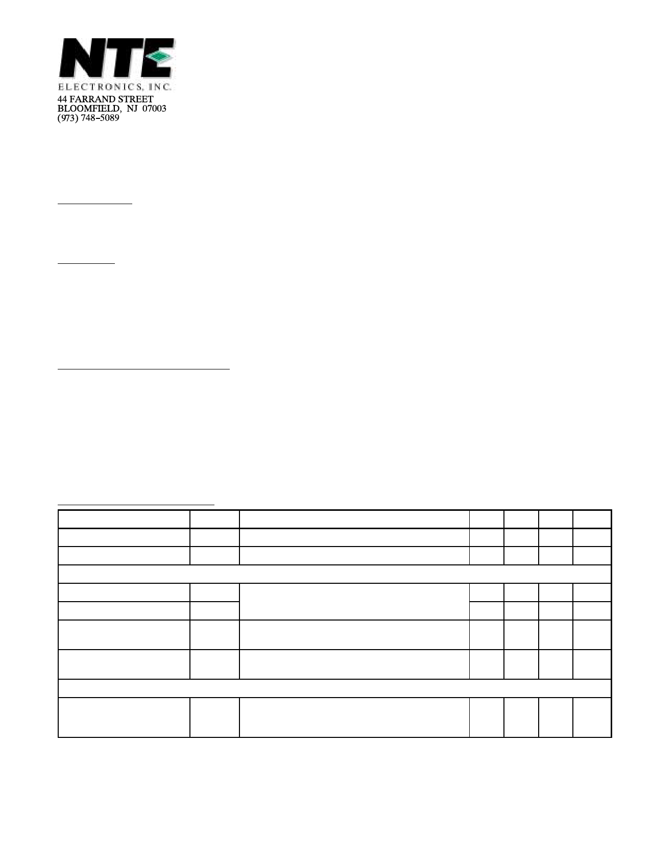
Electrical Characteristics: (TA = +25C, VCC = 12V unless otherwise specified)
Parameter
Symbol
Test Conditions
Min Typ Max Unit
Circuit Current
Circuit Voltage
Volume Circuit
Itot VCC = 12V
24 38 50 mA
V3, 10–7 Vi = No Signal, V12 = VCC, V1 = V5 = V8 = VCC/2 8.0 8.4 8.8
V
Maximum Output
Channel Balance (Note 1)
VOmax f = 1kHz, Vi = 400mVrms, V12 = VCC,
CB
V1 = V5 = V8 = VCC/2
190 230 270 mVrms
– +0.2 ±1.0
Volume Starting Voltage
Residual Tone Level
(Volume Minimum)
Balance Control Circuit
V(st)
Vmin.
f = 1kHz, Vi = 400mVrms, V12 = VR,
V1 = V5 = V8 = VCC/2, Note 2
f = 1kHz, Vi = 400mVrms, V12 = 0,
V1 = V5 = V8 = VCC/2
0.40 0.60 0.90 V
–
25 50 µVrms
Attenuation (R–ch)
AttBR
f = 1kHz, Vi = 400mVrms, V12 = VCC,
V5 = V8 = VCC/2, VOR1: V1 = (5.5/12),
VCC(VR–1), VOR2: V1 = 0V, Note 3
Note 1. Deviation between R and L–ch for maximum output.
Note 2. V12 voltage when output voltage is 0.1mVrms.
Note 3. AttBR: VOR2/VOR1
–32 –45 –
dB
Share Link: 