M29W008AB データシートの表示(PDF) - STMicroelectronics
部品番号
コンポーネント説明
メーカー
M29W008AB Datasheet PDF : 30 Pages
| |||
M29W008AT, M29W008AB
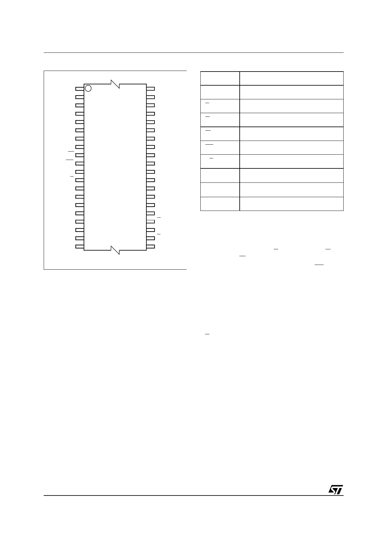
Figure 2. TSOP Connections
A16 1
40 A17
A15
VSS
A14
NC
A13
A19
A12
A10
A11
DQ7
A9
DQ6
A8
DQ5
W
DQ4
RP 10 M29W008AT 31 VCC
NC 11 M29W008AB 30 VCC
RB
NC
A18
DQ3
A7
DQ2
A6
DQ1
A5
DQ0
A4
G
A3
VSS
A2
E
A1 20
21 A0
AI02717
DESCRIPTION
The M29W008A is a non-volatile memory that may
be erased electrically at the block or chip level and
programmed in-system on a Byte-by-Byte basis
using only a single 2.7V to 3.6V VCC supply. For
Program and Erase operations the necessary high
voltages are generated internally. The device can
also be programmed in standard programmers.
The array matrix organisation allows each block to
be erased and reprogrammed without affecting
other blocks. Blocks can be protected against pro-
graming and erase on programming equipment,
and temporarily unprotected to make changes in
the application. Each block can be programmed
and erased over 100,000 cycles.
Instructions for Read/Reset, Auto Select for read-
ing the Electronic Signature or Block Protection
status, Programming, Block and Chip Erase,
Erase Suspend and Resume are written to the de-
vice in cycles of commands to a Command Inter-
face using standard microprocessor write timings.
The device is offered in TSOP40 (10 x 20mm)
package.
Table 1. Signal Names
A0-A19
Address Inputs
DQ0-DQ7 Data Input/Outputs, Command Inputs
E
Chip Enable
G
Output Enable
W
Write Enable
RP
Reset/Block Temporary Unprotect
RB
Ready/Busy Output
VCC
Supply Voltage
VSS
Ground
NC
Not Connected Internally
Organisation
The M29W008A is organised as 1Mb x8. The
memory uses the address inputs A0-A19 and the
Data Input/Outputs DQ0-DQ7. Memory control is
provided by Chip Enable E, Output Enable G and
Write Enable W inputs.
A Reset/Block Temporary Unprotection RP tri-lev-
el input provides a hardware reset when pulled
Low, and when held High (at VID) temporarily un-
protects blocks previously protected allowing them
to be programed and erased. Erase and Program
operations are controlled by an internal Program/
Erase Controller (P/E.C.). Status Register data
output on DQ7 provides a Data Polling signal, and
DQ6 and DQ2 provide Toggle signals to indicate
the state of the P/E.C operations. A Ready/Busy
RB output indicates the completion of the internal
algorithms.
Memory Blocks
The devices feature asymmetrically blocked archi-
tecture providing system memory integration. Both
M29W008AT and M29W008AB devices have an
array of 19 blocks, one Boot Block of 16 Kbytes,
two Parameter Blocks of 8 Kbytes, one Main Block
of 32 Kbytes and fifteen Main Blocks of 64 Kbytes.
The M29W008AT has the Boot Block at the top of
the memory address space and the M29W008AB
locates the Boot Block starting at the bottom. The
memory maps are showed in Tables 3, 4. Each
block can be erased separately, any combination
of blocks can be specified for multi-block erase or
the entire chip may be erased. The Erase opera-
tions are managed automatically by the P/E.C.
2/30
Share Link: 