A6A259KA データシートの表示(PDF) - Allegro MicroSystems
部品番号
コンポーネント説明
メーカー
A6A259KA Datasheet PDF : 10 Pages
| |||
6A259
8-BIT ADDRESSABLE
DMOS POWER DRIVER
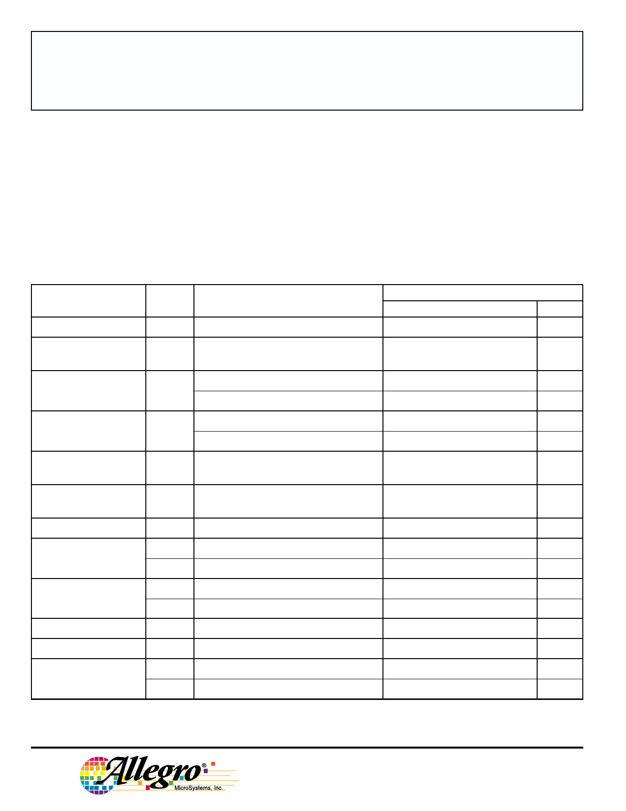
RECOMMENDED OPERATING CONDITIONS
over operating temperature range
Logic Supply Voltage Range, VDD ............... 4.5 V to 5.5 V
High-Level Input Voltage, VIH ............................ ≥ 0.85VDD
Low-level input voltage, VIL ................................. ≤0.15VDD
ELECTRICAL CHARACTERISTICS at TA = +25°C, VDD = 5 V, tir = tif ≤ 10 ns (unless otherwise
specified).
Characteristic
Logic Supply Voltage
Output Breakdown
Voltage
Symbol
VDD
V(BR)DSX
Test Conditions
Operating
IO = 1 mA
Min.
4.5
50
Limits
Typ.
Max.
5.0
5.5
—
—
Units
V
V
Off-State Output
Current
Static Drain-Source
On-State Resistance
Source-to-Drain
Diode Voltage
IDSX
rDS(on)
VSD
VO = 40 V
VO = 40 V, TA = 125°C
IO = 350 mA
IO = 350 mA, TA = 125°C
IF = 350 mA
—
0.1
1.0
µA
—
0.2
5.0
µA
—
1.0
1.5
Ω
—
1.7
2.5
Ω
—
1.0
—
V
Nominal Output
Current
IO(nom) VDS(on) = 0.5 V, TA = 85°C
—
350
—
mA
Output Current
IO(chop) IO at which chopping starts, TC = 25°C
0.6
0.8
1.1
A
Logic Input Current
IIH
VI = VDD = 5.5 V
—
—
1.0
µA
IIL
VI = 0, VDD = 5.5 V
—
—
-1.0
µA
Prop. Delay Time
tPLH
IO = 350 mA, CL = 30 pF
—
100
—
ns
tPHL
IO = 350 mA, CL = 30 pF
—
60
—
ns
Output Rise Time
tr
IO = 350 mA, CL = 30 pF
—
55
—
ns
Output Fall Time
tf
IO = 350 mA, CL = 30 pF
Supply Current
IDD(off) VDD = 5.5 V, Outputs OFF
IDD(on) VDD = 5.5 V, Outputs ON
Typical Data is at VDD = 5 V and is for design information only.
NOTE — Pulse test, duration ≤ 100 µs, duty cycle ≤ 2%.
—
40
—
ns
—
15
100
µA
—
150
300
µA
115 Northeast Cutoff, Box 15036
Worcester, Massachusetts 01615-0036 (508) 853-5000
Share Link: 