PBL38541/1N データシートの表示(PDF) - Ericsson
部品番号
コンポーネント説明
メーカー
PBL38541/1N Datasheet PDF : 14 Pages
| |||
PBL 385 41
Note that the signals at points a. and b. are
180 degrees off phase.
10 x R6 ≈ R7 + Zbal Note #1
R7 ≈ Zbal
Note#2
The ac-signal at point c. is now 1/10 of the
signal on the line because it is further
divided by two from point b. (R7≈Zbal).
Hence 10 x R10 ≈ R11 to satisfy the
balancing criteria. R12 is to set the receiver
gain. ( can also be a volume control potentio-
meter).
Note #1 These values ensure that the
frequency behaviour of the transmitter is
minimal. With the ratio 1/10 the influence
is 1 dB, and with ratio 1/20 it´s 0.5 dB.
Note #2 If the R7 is made low ohmic
compared with Zbal, it will load the latter
and result in a bad side tone
perfomannce, again if the R7 is made high
ohmic compared with Zbal will result in a
low signal to balance the side tone with and
make the balancing difficult. Making any of
the impedances unnecessary high will
make the circuit sensitive to RFI. All values
given here are approximate and serve as
starting entities only. The final trimming
of side tone network is a cut and try propo-
sition because a part of the balance lies
in the acoustical path between the
microphone and earphone.
Reverse side tone network.
This type of side tone balancing will
help when for some reason there is a need
to make the R6 low < 47Ω and thus the
signal for balancing gets small across R6.
By placing the balancing network like shown
in fig.15 the possible signal level is 6 dB
higher than in the first case and it will also
help in case when a volume control is
added to the receiver.
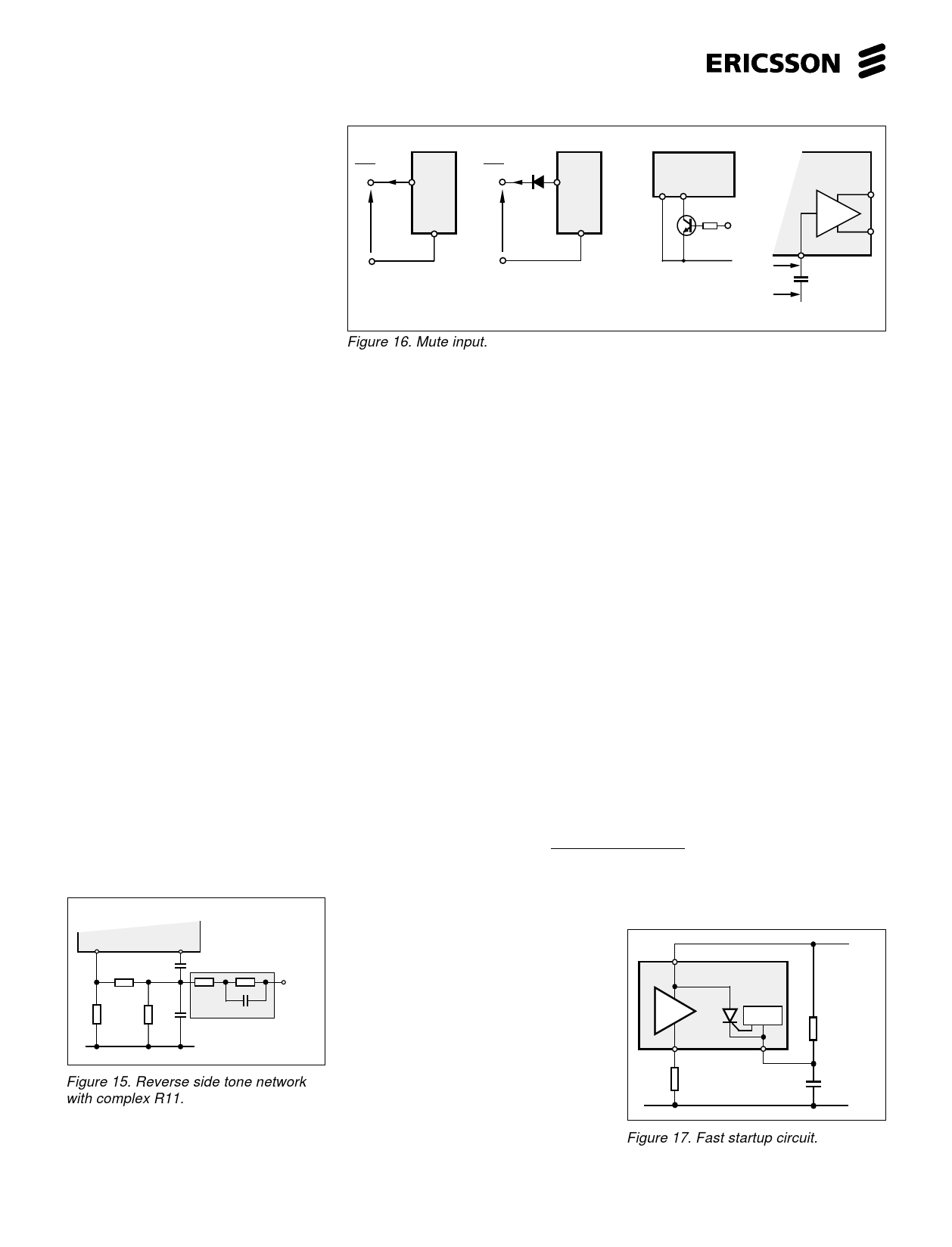
a)
Mute IMute
PBL
38541
5
VMute
14
-L
b)
Mute IMute
PBL
38541
5
VMute
14
-L
The diode has to be low
voltage drop type.
Figure 16. Mute input.
Mute function.
The circuit has a mute function at pin 5.
Sinking current from this pin will cut off the
gain in the microphone amplifier
(attenuation min. 60dB) and decrease the
gain in the receiver amplifier to reach the
confidence tone level at DTMF-dialling.
The receiver mute is ≈ 40dB down from the
unmuted value to satisfy those who keep
the handset close to the ear at dialling. The
mute signal also switches the output at pin
11 from microphone amplifier output to the
signaling amplifier (payphone and DTMF
signals) output.
Optional conditions.
For users who keep the handset from
the ear the confidence tone level is too low.
To alter the level, a signal can be taken
from DTMF generator output to receiver
input before the capacitor C6. The added
impedance to this point will hardly disturbe
the signal condition in active speech mode.
The microphone amplifier only, can be
muted by sinking current from the output
pin 11.
c)
PBL
38541
14 5
-L
Mute
d)
PBL
38541
17
Rx
18
15
Muting
points
Receiver mute only.
Figure 16 b.) If the system mute
signal is used to other tasks than muting
the speech circuit it has to be isolated. If a
diode is used it has to be a low voltage
drop type. The input at mute has to be
below 300mV. If the mute signal has
reverse polarity out of the system it can be
phase changed like in c.) In case it is
required to mute the receiver only, d.) it
can be done by shorting the receiver input
to ground before or after the input capacitor.
Shorting the input pin to ground (does not
have to be absolute ground) actuates a
mute by driving the amplifier into saturation
thus blocking the signal path and rende-
ring a mute with high attenuation but will
cause a DC-level shift at output which in
its turn will cause a ”click ” in the earphone.
This can be softened with a slower mute
signal flank. If the second approach,
grounding before the input capacitor is
chosen, the grounding has to be low ohmic
in order to render a high attenuating mute.
PBL 385 41
2
15
C6
R10
R6
R12
R11
Z bal.
C*
* To give receiver flat
frequency response
+Line
Figure 15. Reverse side tone network
with complex R11.
10
Start up circuit
The circuit contains a start up device
which function is to fast charge capacitor
C1 when the circuit goes into hook- off
condition. The fast charge circuit is a
thyristor function between pins 1 and 4 that
will stop conducting when the current drain
at pin 4 is lower than ≈ 700 µA + the internal
current consumption ( about 1 mA). Care
must be taken when connecting external
load to pin 4 in order not to exeed the ≈ 700
µA limit. Should this happen, it would result
in an inoperative speech funktion. This
circuit can not retrigger before the voltage
level at C1 drops below 2V or the line
voltage is below 1V. See fig. 17.
1
PBL 385 41
+Line
Tx
2
R6
DC supply
4
R3
+
C1
-Line
Figure 17. Fast startup circuit.
Share Link: 