PC85132/232-1 データシートの表示(PDF) - NXP Semiconductors.
部品番号
コンポーネント説明
メーカー
PC85132/232-1 Datasheet PDF : 65 Pages
| |||
NXP Semiconductors
PCA85132
LCD driver for low multiplex rates
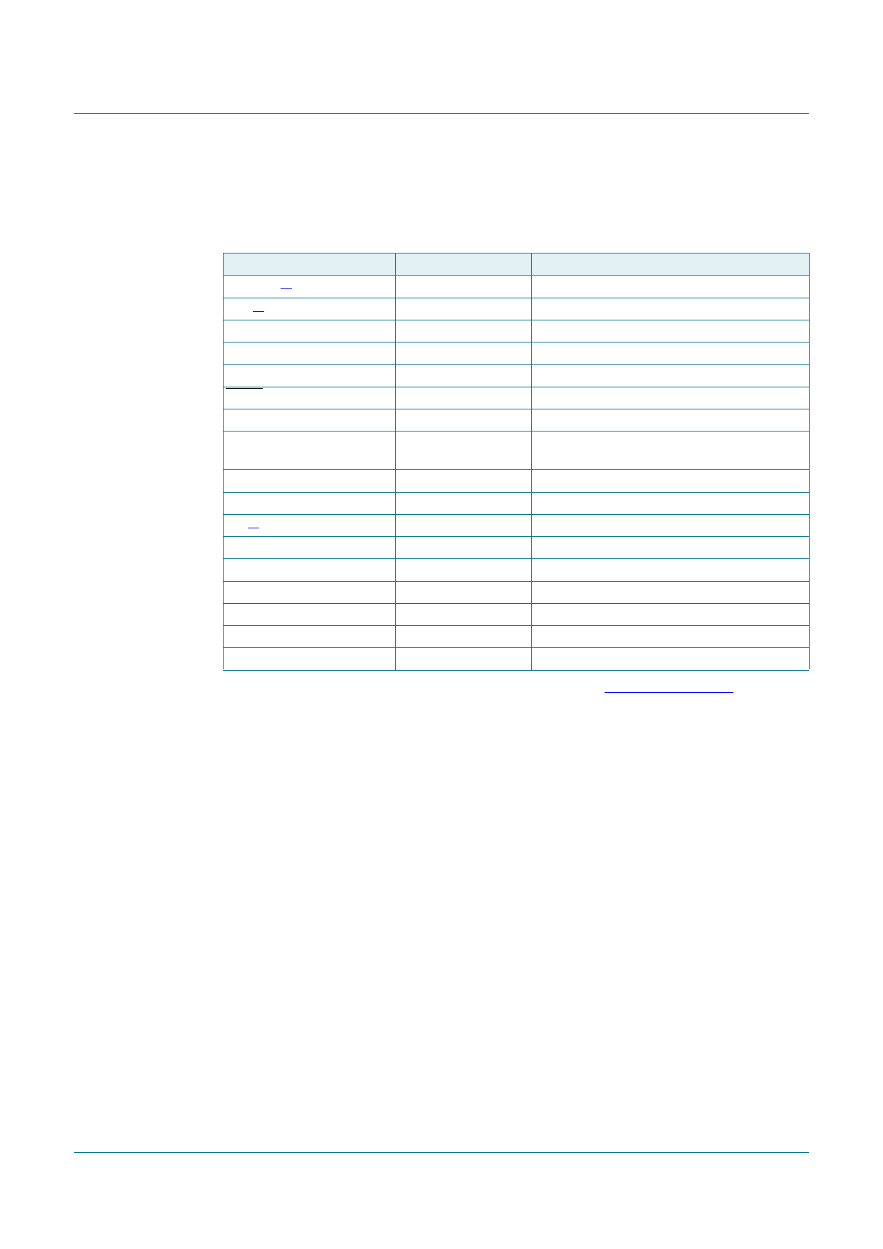
6.2 Pin description
Table 4. Pin description
Input or input/output pins must always be at a defined level (VSS or VDD) unless otherwise specified.
Symbol
Pin
Description
SDAACK[1]
1 to 3
I2C-bus acknowledge output
SDA[1]
4 to 6
I2C-bus serial data input
SCL
7 to 9
I2C-bus serial clock input
CLK
10
clock input and output
VDD
SYNC
11 to 13
14
supply voltage
cascade synchronization input and output
OSC
15
selection of internal or external clock
T1, T2, and T3
16, 17, and 18 to 20 dedicated testing pins; to be tied to VSS in
application mode
A0 and A1
21, 22
subaddress inputs
SA0
23
I2C-bus slave address input
VSS[2]
VLCD
BP2 and BP0
24 to 26
27 to 29
30, 31
ground supply voltage
LCD supply voltage
LCD backplane outputs
S0 to S79
32 to 111
LCD segment outputs
BP0, BP2, BP1, and BP3 112 to 115
LCD backplane outputs
S80 to S159
116 to 195
LCD segment outputs
BP3 and BP1
196, 197
LCD backplane outputs
[1] For most applications SDA and SDAACK are shorted together (see Section 14.3 on page 44).
[2] The substrate (rear side of the die) is connected to VSS and should be electrically isolated.
PCA85132
Product data sheet
All information provided in this document is subject to legal disclaimers.
Rev. 4 — 9 April 2015
© NXP Semiconductors N.V. 2015. All rights reserved.
5 of 65
Share Link: 