9532 гГЗгГЉгВњгВЈгГЉгГИгБЃи°®з§ЇпЉИPDFпЉЙ - Philips Electronics
йГ®еУБзХ™еПЈ
гВ≥гГ≥гГЭгГЉгГНгГ≥гГИи™ђжШО
гГ°гГЉгВЂгГЉ
9532 Datasheet PDF : 20 Pages
| |||
Philips Semiconductors
16-bit I2C LED dimmer
Product data
PCA9532
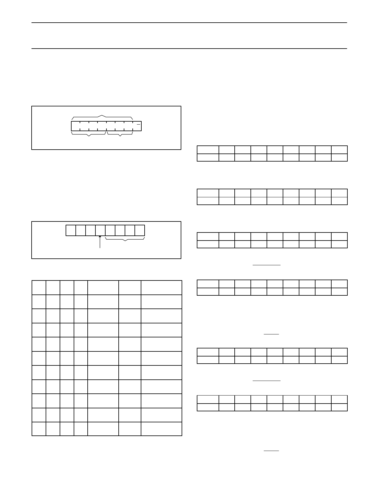
DEVICE ADDRESSING
Following a START condition the bus master must output the
address of the slave it is accessing. The address of the PCA9532 is
shown in Figure 4. To conserve power, no internal pull-up resistors
are incorporated on the hardware selectable address pins and they
must be pulled HIGH or LOW.
SLAVE ADDRESS
1 1 0 0 A2 A1 A0 R/W
FIXED
HARDWARE SELECTABLE
su01420
Figure 4. Slave address
The last bit of the address byte defines the operation to be
performed. When set to logic 1 a read is selected while a logic 0
selects a write operation.
CONTROL REGISTER
Following the successful acknowledgement of the slave address,
the bus master will send a byte to the PCA9532 which will be stored
in the Control Register. This register can be read and written via the
I2C-bus.
0 0 0 AI B3 B2 B1 B0
RESET STATE: 00h
REGISTER ADDRESS
AUTO-INCREMENT FLAG
Figure 5. Control register
SW00898
CONTROL REGISTER DEFINITION
B3
B2
B1
B0
REGISTER
NAME
TYPE
REGISTER
FUNCTION
0
00
0
INPUT0
READ
INPUT
REGISTER 0
0
00
1
INPUT1
READ
INPUT
REGISTER 1
0010
PSC0
READ/ FREQUENCY
WRITE PRESCALER 0
0011
PWM0
READ/
PWM
WRITE REGISTER 0
0100
PSC1
READ/ FREQUENCY
WRITE PRESCALER 1
0101
PWM1
READ/
PWM
WRITE REGISTER 1
0110
LS0
READ/
WRITE
LED 0-3
SELECTOR
0111
LS1
READ/
WRITE
LED 4-7
SELECTOR
1000
LS2
READ/
WRITE
LED 8-11
SELECTOR
1001
LS3
READ/
WRITE
LED 12-15
SELECTOR
REGISTER DESCRIPTION
The lowest 3 bits are used as a pointer to determine which register
will be accessed.
If the auto-increment flag (AI) is set, the four low order bits of the
Control Register are automatically incremented after a read or write.
This allows the user to program the registers sequentially. The
contents of these bits will rollover to вАШ0000вАЩ after the last register is
accessed.
When auto-increment flag is set (AI = 1) and a read sequence is
initiated, the sequence must start by reading a register different from
вАШ0вАЩ (B3 B2 B1 B0 0 0 0 0 0)
Only the 4 least significant bits are affected by the AI flag.
Unused bits must be programmed with zeroes.
INPUT0 вАФ INPUT REGISTER 1
bit
I7 I6 I5 I4 I3 I2 I1 I0
default 0
0
0
0
0
0
0
0
The INPUT register 1 reflects the state of the device pins (inputs 0
to 7). Writes to this register will be acknowledged but will have no
effect.
INPUT1 вАФ INPUT REGISTER 2
bit I15 I14 I13 I12 I11 I10 I9 I8
default 0
0
0
0
0
0
0
0
The INPUT register 1 reflects the state of the device pins (inputs 8
to 15). Writes to this register will be acknowledged but will have no
effect.
PSC0 вАФ FREQUENCY PRESCALER 0
bit
7
6
5
4
3
2
1
0
default 0
0
0
0
0
0
0
0
PSC0 is used to program the period of the PWM output.
The
period
of
BLINK0
+
(PSC0 ) 1)
152
PWM0 вАФ PWM REGISTER 0
bit
7
6
5
4
3
2
1
0
default 1
0
0
0
0
0
0
0
The PWM0 register determines the duty cycle of BLINK0. The
outputs are LOW (LED on) when the count is less than the value in
PWM0 and HIGH (LED off) when it is greater. If PWM0 is
programmed with 00h, then the PWM0 output is always HIGH
(LED off).
The duty cycle of BLINK0 is:
PWM0
256
PSC1 вАФ FREQUENCY PRESCALER 1
bit
7
6
5
4
3
2
1
0
default 0
0
0
0
0
0
0
0
PSC1 is used to program the period of PWM output.
The
period
of
BLINK1
+
(PSC1 ) 1)
152
PWM1 вАФ PWM REGISTER 1
bit
7
6
5
4
3
2
1
0
default 1
0
0
0
0
0
0
0
The PWM1 register determines the duty cycle of BLINK1. The
outputs are LOW (LED on) when the count is less than the value in
PWM1 and HIGH (LED off) when it is greater. If PWM1 is
programmed with 00h, then the PWM1 output is always HIGH
(LED off).
The duty cycle of BLINK1 is:
PWM1
256
2003 May 02
5
Share Link: 