PCA9541PW データシートの表示(PDF) - NXP Semiconductors.
部品番号
コンポーネント説明
メーカー
PCA9541PW Datasheet PDF : 41 Pages
| |||
NXP Semiconductors
PCA9541
2-to-1 I2C-bus master selector with interrupt logic and reset
The MYTEST and the NMYTEST bits cause the interrupt pins of the respective masters to
be activated for a ‘functional interrupt test’.
Remark: The regular way to proceed is that a master asks to take the control of the bus
by programming MYBUS and BUSON bits based on NMUYBUS and NBUSON values.
Nevertheless, the same master can also decide to give up the control of the bus and give
it to the other master. This is also done by programming the MYBUS and BUSON bits
based on NMYBUS and NBUSON values.
Remark: Any writes either to the Interrupt Enable Register or the Control Register cause
the respective register to be updated on the 9th clock cycle, that is, on the rising edge of
the acknowledge clock cycle.
Remark: The actual switch from one channel to another or the switching off of both the
channels happens on a STOP command that is sent by the master requesting the switch.
8.3.1 Register 0: Interrupt Enable (IE) register (B1:B0 = 00b)
This register allows a master to read and/or write (if needed) Mask options for its own
channel.
The Interrupt Enable register described below is identical for both the masters.
Nevertheless, there are physically 2 internal Interrupt Enable registers, one for each
upstream channel. When Master 0 reads/writes in this register, the internal Interrupt
Enable Register 0 will be accessed. When Master 1 reads/writes in this register, the
internal Interrupt Enable Register 1 will be accessed.
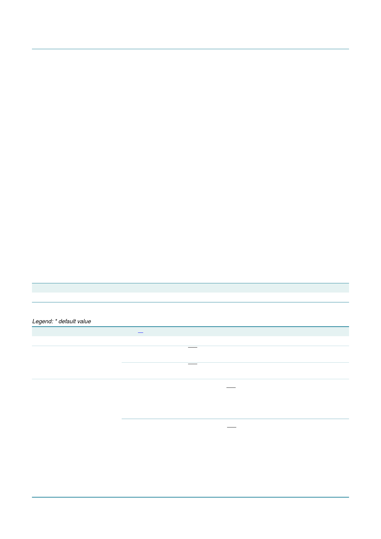
Table 5.
7
0
Register 0 - Interrupt Enable (IE) register (B1:B0 = 00b) bit allocation
6
5
4
3
2
0
0
0
BUSLOSTMSK BUSOKMSK
1
BUSINITMSK
0
INTINMSK
Table 6. Register 0 - Interrupt Enable (IE) register bit description
Legend: * default value
Bit Symbol
Access Value[1] Description
7:4 -
R only 0*
not used
3
BUSLOSTMSK R/W 0*
An interrupt on INT will be generated after the other master has been
disconnected.
1
An interrupt on INT will not be generated after the other master has been
disconnected.
2
BUSOKMSK R/W 0*
After connection is requested and Bus Initialization not requested
(BUSINIT = 0), an interrupt on INT will be generated when a non-idle situation
has been detected on the downstream slave channel by the bus sensor at the
switching moment.
Remark: Channel switching is done automatically after the STOP command.
1
After connection is requested and Bus Initialization not requested
(BUSINIT = 0), an interrupt on INT will not be generated when a non-idle
situation has been detected on the downstream slave channel by the bus
sensor at the switching moment (masked).
Remark: Channel switching is done automatically after the STOP command.
PCA9541_7
Product data sheet
Rev. 07 — 2 July 2009
© NXP B.V. 2009. All rights reserved.
10 of 41
Share Link: 